Lecture 19
Andreas Moshovos
Spring 2007
Implementing a Simple
CPU
We now switch topics. We assume that there is an understanding of how CPUs behave which is sufficient for programming them. This is the role of the computer user/programmer. In what follows we switch roles and assume the role of the computer designer. This is the person that designs a piece of hardware, the CPU that behaves exactly the way the programmer expects it will. Recall, that the behavior model of the CPU is the contract between the designer and the programmer. Thus it allows the two parties to proceed independently.
We will three different methodologies for implementing CPUs. The textbook presents one of these styles. This will be the last one that we will present during our lectures. For clarity, we will restrict our attention to a hypothetical, simple CPU.
Instruction Set
Definition
We will use the following instruction set/behavior model for our examples. Assume a hypothetical architecture where there are just 256 memory locations. Our CPU has four general purpose registers called K0 through K3 each capable of storing just 8 bits. The CPU also has a PC register which is also 8 bits. Upon resetting the CPU (e.g., power up), the PC takes the value $80. Our CPU does not support interrupts. In addition, there are two condition code bits Z = zero and N = negative.
Our CPU is capable of executing the following 10 instructions:
LOAD R1 (R2):
TMP = MEM [R2]
R1 = TMP
PC = PC + 1
STORE R1 (R2):
MEM [R2] = R1
PC = PC + 1
ADD R1 R2
TMP = R1 + R2
R1 = TMP
IF (TMP == 0) ZERO = 1; ELSE ZERO =
0;
IF (TMP < 0) NEGATIVE = 1; ELSE
NEGATIVE = 0;
PC = PC + 1
SUB R1 R2
TMP = R1 - R2
R1 = TMP
IF (TMP == 0) ZERO = 1; ELSE ZERO =
0;
IF (TMP < 0) NEGATIVE = 1; ELSE
NEGATIVE = 0;
PC = PC + 1
NAND R1 R2
TMP = R1 bitwise NAND R2
R1 = TMP
IF (TMP == 0) ZERO = 1; ELSE ZERO =
0;
IF (TMP < 0) NEGATIVE = 1; ELSE
NEGATIVE = 0;
PC = PC + 1
ORI IMM5
TMP = Κ1 bitwise OR IMM5, where IMM5 is a 5 bit constant
Κ1 = TMP
IF (TMP == 0) ZERO = 1; ELSE ZERO =
0;
IF (TMP < 0) NEGATIVE = 1; ELSE
NEGATIVE = 0;
PC = PC + 1
SHIFT L/R R1 ΙΜΜ2
IF
(L) ΤΗΕΝ TMP = R1 << IMM2
ELSE TMP = R1 >> IMM2
R1 = TMP
IF
(TMP == 0) ZERO = 1; ELSE ZERO = 0;
IF
(TMP < 0) NEGATIVE = 1; ELSE NEGATIVE = 0;
PC
= PC + 1
Alternative
definition (equivalent to the previous one):
ΙΜΜ3
is
a 3 bit immediate in the sign – magnitude representation, i.e., bit 2 = sign, value = bits 1 and 0
IF (IMM3 > 0) ΤΗΕΝ TMP = R1 << IMM3
ELSE TMP = R1 >> (-IMM3)
R1 = TMP
IF
(TMP == 0) ZERO = 1; ELSE ZERO = 0;
IF
(TMP < 0) NEGATIVE = 1; ELSE NEGATIVE = 0;
PC
= PC + 1
BZ IMM4
where ΙΜΜ4 is a 2’s complement 4-bit immediate
IF
(ZERO == 1) PC = PC + 1 + (SIGN-EXTEND8(IMM4))
ELSE PC = PC + 1
BNZ IMM4
IMM4 as in BZ
IF
(ZERO == 0) PC = PC + 1 + (SIGN-EXTEND8(IMM4))
ELSE PC = PC + 1
BPZ IMM4
IMM4 as in BZ
IF
(NEGATIVE == 0) PC = PC + 1 + (SIGN-EXTEND8(IMM4))
ELSE PC = PC + 1
Each instruction is encoded in one byte as follows:
LOAD
|
7 |
6 |
5 |
4 |
3 |
2 |
1 |
0 |
|
R1 |
R1 |
R2 |
R2 |
0 |
0 |
0 |
0 |
STORE
|
7 |
6 |
5 |
4 |
3 |
2 |
1 |
0 |
|
R1 |
R1 |
R2 |
R2 |
0 |
0 |
1 |
0 |
ADD
|
7 |
6 |
5 |
4 |
3 |
2 |
1 |
0 |
|
R1 |
R1 |
R2 |
R2 |
0 |
1 |
0 |
0 |
SUB
|
7 |
6 |
5 |
4 |
3 |
2 |
1 |
0 |
|
R1 |
R1 |
R2 |
R2 |
0 |
1 |
1 |
0 |
NAND
|
7 |
6 |
5 |
4 |
3 |
2 |
1 |
0 |
|
R1 |
R1 |
R2 |
R2 |
1 |
0 |
0 |
0 |
ORI
|
7 |
6 |
5 |
4 |
3 |
2 |
1 |
0 |
|
IMM5_4 |
IMM5_3 |
IMM5_2 |
IMM5_1 |
IMM5_0 |
1 |
1 |
1 |
SHIFT
|
7 |
6 |
5 |
4 |
3 |
2 |
1 |
0 |
|
R1 |
R1 |
L/!R |
IMM2_1 |
IMM2_0 |
0 |
1 |
1 |
BZ
|
7 |
6 |
5 |
4 |
3 |
2 |
1 |
0 |
|
IMM4_3 |
IMM4_2 |
IMM4_1 |
IMM4_0 |
0 |
1 |
0 |
1 |
BNZ
|
7 |
6 |
5 |
4 |
3 |
2 |
1 |
0 |
|
IMM4_3 |
IMM4_2 |
IMM4_1 |
IMM4_0 |
1 |
0 |
0 |
1 |
BPZ
|
7 |
6 |
5 |
4 |
3 |
2 |
1 |
0 |
|
IMM4_3 |
IMM4_2 |
IMM4_1 |
IMM4_0 |
1 |
1 |
0 |
1 |
A few examples:
“Add k2 k1” is encoded as %10 01 0100, where the first 10
refers to register
“Load k3 (k1)” is encoded as %11 01 0000, 11 for k3, 01 for k1 and 0000 for load. This reads from the memory location given by the value of k1 and writes the value read into k3.
%10100111 decodes to “ORI $14”, since the last three bits are 111 which corresponds to ORI and the rest are 1 0100 which is the number $14.
%10010110 decodes to “SUB K2, K1” since the last four bits are 0110 which corresponds to SUB and then the upper two bits mean K2 and the next two bits mean K1.
Datapath and Control
Generally speaking an implementation of a CPU can be broken into the implementation of two cooperating units: the datapath and the control.
The datapath is the unit that contains all the registers and the functional units. It is where all data computations take place. The datapath should be constructed in a way such that it is possible to perform all actions necessary to compute the data results of instruction execution. For example, to implement the add instruction the datapath should provide us with the capability of reading the two registers that we want to add, it should have a functional unit that performs the addition and then allow us to write the result back into the appropriate register. We will shortly present a methodology for designing the datapth.
The control orchestrates the actions that take place in the datapath. We will eventually explain that the control is a “giant” finite-state machine that implements the fundamental execution loop: (1) fetch instruction, (2) decode, (3) read source operands, (4) perform operation, (5) store result, (6) determine which instruction to execute next. It does so by instructing the datapath to perform all appropriate actions.
But both concepts are best understood by means of an example.
We will focus on explaining how to design the datapath and then the control.
Single-Cycle
Implementation – General Observations
Our CPU will be implemented as a sequential circuit. That is, it is going to use a clock reference. A clock is a periodic signal that alternates between 0 and 1. This is what they refer to as the clock frequency of the CPU. For example, at the time of this writing the maximum clock frequency for a P4 CPU is 3.8Ghz. This is how the clock signal typically looks like in time (the diagram defines “cycle”, “falling” and “rising” “edges”):
|
TIME ---------------> |
||||||||
|
|
|
|
|
|
|
|
|
|
|
|
|
|
|
|
|
|
|
|
|
|
|
|
|
|
|
|
|
|
|
Falling edge -> |
<------- cycle -------> |
|
<---- rising edge |
|
|
|||
For the first implementation we will present it is important to explain our clocking strategy. In our implementation each instruction will be executed in its entirety within a single cycle. This is why we will refer to this implementation as a single-cycle implementation.
For all storage elements inside and outside our CPU we will assume that reads are done using combinatorial logic (i.e., we can read at any time we wish) but changes happen only at the falling edge of the clock. Our implementation will be such that instruction execution will commence immediately after the falling edge of the clock, during the clock cycle using combinatorial logic we will compute all necessary values and final state changes (in registers or memory) will happen at the very end just when the next falling edge occurs. Our clock cycle will be determined by the delay of the slowest to compute instruction. More on this later on.
Single-Cycle
Implementation – The Datapath
As we mentioned before our goal here is to design a digital circuit that is capable of performing all possible calculations that may be required by any instruction. The methodology that we will follow here is to design a datapath for each instruction separately and then we will combine all circuits together by reusing as much as possible. Before we start designing our datapath let us first present our building blocks. These are supposed to be digital circuits that we know how to build.
Registers
The first building block is a register. A register is a collection of D flip-flops that we can either read or write. In our case, since all registers inside our machine are 8-bit wide, we will be using 8-bit registers. Schematically, a register will be represented as follows:
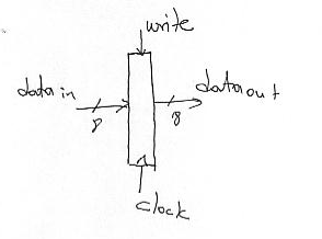
The dataout wires give us the value inside the register. If we want to change this value we need to provide the new value on the datain wires and set the “write” signal to 1. The change will happen on the next falling edge of the clock signal. For clarity we will not draw the clock signal and connections in our diagrams.
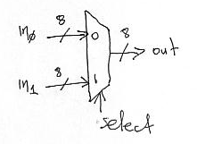
Multiplexers
We are also going to use multiplexers. The following figure illustrates an 8-bit 2-to-1 multiplexer. This is a circuit that accepts two 8-bit inputs, in0 and in1 and produces a single 8-bit output “out”. “out” takes the value of “in0” if the select signal is 0, otherwise it takes the value of “in1”. In general, there could be 2^N input connections in which case the select will be N-wires wide. Depending on what is the value formed on the select input, one of the 2^N inputs will be propagated to the output.
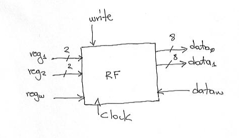
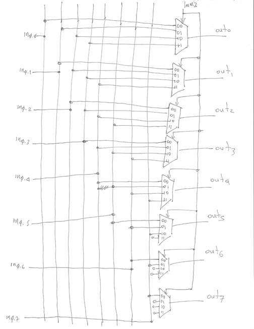
Register File
The register file is where registers K0 through K3 are implemented. Internally, it has four 8 bit registers. Its external interface is illustrated below. It accepts two 2-bit input signals reg1 and reg2. These are used to read two registers simultaneously. We use 2 bit signals since there are four registers. Thus with 2 bits we can uniquely identify each one. The values read are placed on the output signals data0 and data1. These are 8-bit wide since our registers are 8-bit wide.
Our register file also supports a write operation. To write a register we need to specify its name on the regw input, the value we want to write on the dataw 8-bit input and set the “write” signal to 1. The actual write will happen on the next falling edge. For this reason there is a clock connection, however, for clarity we will not draw the clock signal in our diagrams.
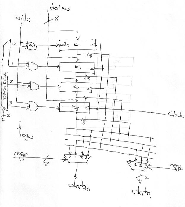
The following figure shows one possible implementation of the register file that uses registers, multiplexers and a decoder:
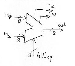
ALU = Arithmetic
Logic Unit
Most calculations will take place in the ALU. The ALU has the following interface. It accepts two 8-bit inputs in0 and in1 and performs the calculation specified by the ALUop signal. For our architecture we need to do addition, subtraction, OR, NAND, and Shift. Thus we need to be able to specify one of these five operations, It is for this reason that the ALUop signal is 3-bits wide. We will use the following mapping of operations to ALUop encoding: 000 = addition, 001 = subtraction, 010 = OR, 011 = NAND, and 100 = Shift. The other three combinations will be reserved for future expansion. The result is placed on the “out” signals. Two additional single bit results are produced N and Z. Z is set to 1 if the value on out is zero. N is set to 1 if out7 (the 8th bit of the out signal) is 1, that is if the result would be negative if it were interpreted as a 2’s complement number.
At some places we may use simpler ALUs that do for example addition. We will clarify these whenever necessary.
There are many different ways of implementing the ALU. A simple to describe implementation uses a collection of functional units. Each functional unit computes independently one of the 5 different operations and a MUX at the output selects the one we want. Here’s the diagram:
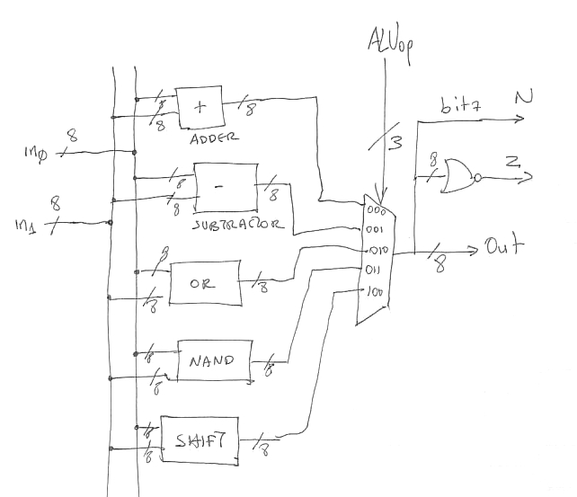
You have seen how to build an 8-bit adder and subtractor in digital design. The OR and NAND boxes contain just eight OR and NAND gates respectively. The SHIFT box is bit more interesting. Here’s one implementation. We break it into two subunits, one for shifting left and another for shifting right. Bits 1..0 of in1 specify by how many bits, whereas bit 2 selects the direction of the shift:
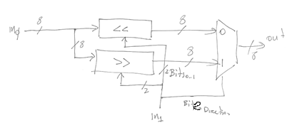
Here’s the diagram for the Shift Left box (<< in the previous figure):
The shift right box is similar. We could have used 8-to-1 multiplexers and implemented both boxes together. Another implementation of shifters is the BARREL SHIFTER. This implementation exploits the observation that a shift by N can be implemented as a series of shifts each by a different power of two. For example, if N is 5 in decimal or 101 in binary, then shifting by 5 bit positions can be achieved by first shifting by 1 bit and then by another 4. Here’s the diagram for a 8-bit left barrel shifter that can shift by 0, 1, 2, or 3 bit positions:

There are two layers of 2-to-1 muxes. The first layer shown in grey uses the least significant bit of the “shift by # of bits” number to either pass the inputs directly or to shift them by 1 bit. The second layer takes the input from the first layer and either passes it as-is or shifts it by 2 bit positions. Hopefully, you will be able to extend this diagram to cope with shifting by larger amounts.
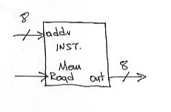
Instruction Memory
We will also need memory. In this implementation we will use two separate memories. One for instructions and one for data. This is commonly referred to as a Harvard Architecture. Most processors that exist today have one memory. However, this implementation is still valid since as we will later see, by using caches it is possible to provide the illusion of separate data and instruction memories. We will later see different implementation methodologies that use just a single memory device. However, these implementation will require multiple cycles to execute a single instruction.
Here’s the interface for instruction memory. It accepts a 8-bit address and after a while it produces the contents of that memory location on the out wires (8 bits too). There is a single control signal, Read, if it is 1 then we are performing a read. Note that in our architecture it is impossible to write to instruction memory.
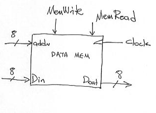
Data Memory
Our data memory is capable of both reads and writes. It presents the following interface. There are two control signals MemRead and MemWrite. If the corresponding signal is set to 1 then we read and write respectively. Only one of them can be activated at any given point in time. Writes happen on the falling edge. In both cases the address we are accessing is given on the addr lines. If we read, memory is going to return the referenced value on the Dout lines. If we write we need to place the value we want on the Din lines.
Other components
We will also need single flip-flops for the N and Z bits.
Designing the Datapath
We are now ready to explain how we can design the datapath. Recall our goal is to produce a circuit that is capable of performing all actions necessary to perform any instruction. Thus one way of doing this is to design a “datapath” for each instruction separately and then combine these together with appropriate glue logic. Let’s start with the add instruction.
Datapath for ADD:
No matter the instruction we need to first fetch its representation from instruction memory. This part is actually common for any instruction. Here’s the circuit for doing this:
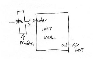
We just connect the output of the PC register to the address lines of instruction memory. Thus, after a while on the INST wires (8-bits) we will get the value stored at the memory location pointed to by PC. This is the next instruction to execute. Assuming that this is an ADD then it will have the following form:
ADD
|
7 |
6 |
5 |
4 |
3 |
2 |
1 |
0 |
|
R1 |
R1 |
R2 |
R2 |
0 |
1 |
0 |
0 |
Bit
0 will appear on wire INST0 and so on. So bits INST3 through INST0 will form
the value 0100 if this is indeed an ADD (the control will look at this as we
will later see). Once we read the instruction representation its time to
execute the instruction. What needs to take place is clearly defined by the
behavior model of the add instruction:
TMP = R1 + R2
R1 = TMP
IF (TMP == 0) ZERO = 1; ELSE ZERO =
0;
IF (TMP < 0) NEGATIVE = 1; ELSE
NEGATIVE = 0;
PC = PC + 1
We
will need to read the two registers add them together and write the result back
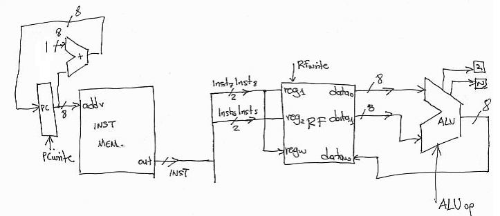
into the register file. Here’s the circuit:
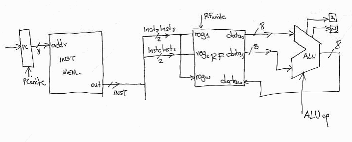
Note
that we use the 7th and 6th bit of INST to drive the reg1
and regw register selection signals. This way we are
reading the register R1 as specified in the instruction encoding. This is both
a source and a destination for us. We use bits 5 and 6 of INST to drive the
second register selection signal reg2. This way we read the second register. We
drive the two register value to the ALU where we have to make sure that we set
the ALUop signal for performing addition. After a
while, the ALU out will have the sum of the two register values. By setting the
RFwrite signal this sum will be written into R1
(since the R1 bits from INST are connected to regw)
on the next falling edge. We assume that
the Z and N flags are also set accordingly by the ALU and will change also on
the next falling edge.
We
are not done. We also need to increment the PC since in the next cycle we need to
execute the next in memory instruction. This is done by using a dedicated
adder. Thus the complete datapath for add looks as
follows:
Datapath for SUB and NAND:
The datapath for SUB and NAND is identical to that for ADD. The only difference is that the ALUop signal needs to be set to different values so that the appropriate calculation takes place (subtraction or bitwise NAND).
Datapath for ORI:
This is very similar to ADD, SUB and NAND. The major difference is that the ORI instruction uses an immediate field as its second operand (i.e., it does not read two registers). So, we can augment our datapath to also support the ORI instruction by placing a mux in front of the second ALU input. This way we can select either the output from the register file or the Imm5 field from the instruction (wires INST7 through INST3):
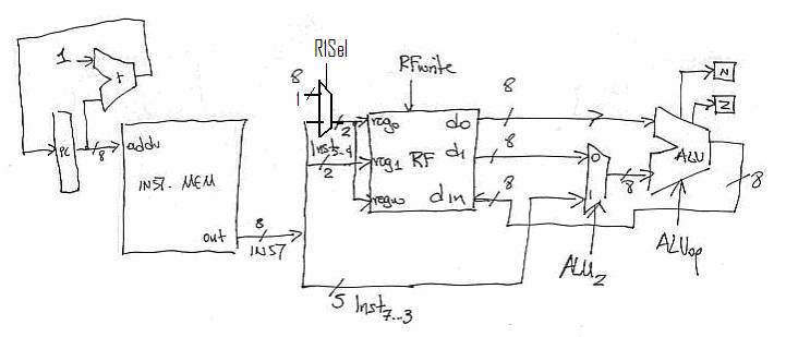
Notice that we introduced a MUX and a control signal ALU2. This way by setting ALU2 to 0 we can implement the datapath for ADD, SUB and NAND. If we set it to 1 we get the datapath for ORI. We directly connect the Imm5 field from the INST wires since it is there that it will appear. Finally, notice that we still read two registers from the register file. However, we only care for one of them (reg0). This is OK as reads are not destructive. If we wanted to avoid this we would need additional control signals in the register file to inhibit reads.
The ORI instruction uses *implied* source and destination registers.
Accordingly we need to augment the previous datapath
providing the capability of directly specifying K1 as a source (R1 at port
reg1) and as destination (R1 at port regw). For this
a mux is sufficient as shown in the diagram that
follows:
Datapath for Branch Instructions:
To implement branches we need to set PC to either PC+1 or to PC + sign-extend(Imm4). The Imm4 comes embedded into the instruction. We need to first sign extend this immediate to 8 bits. Here’s the “circuit”:
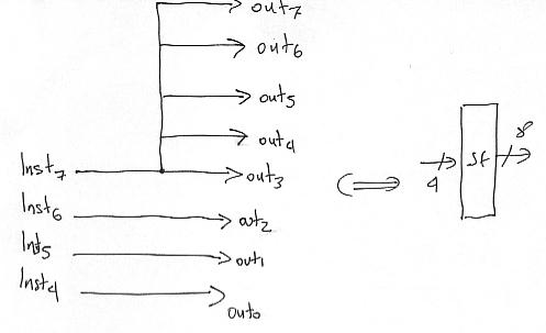
We will the symbol on the right. It turns out that all we need is just wires. We are replicating the sign bit.
To support branch instruction we need to augment the datapath portion that drives the PC register. To do so, we calculate PC+1 as before but in addition we also calculate PC + sign-extend(Imm4). We introduce a multiplexer to allow the PC to be written into with one of these two results as follows:
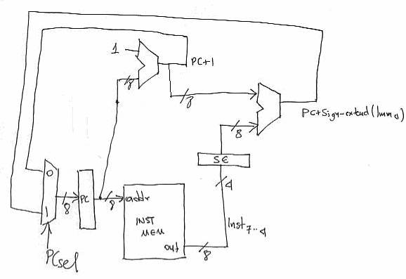 (Corrected:
Calculates PC + Imm4 + 1 as opposed to PC + Imm4)
(Corrected:
Calculates PC + Imm4 + 1 as opposed to PC + Imm4)
By setting the PCsel signal the control can now either assign PC to PC+1 or to PC+Imm4. When we design the control we will see how this decision can be made based on the Z and N flag values. Note that we only showed the PC datapth the rest is still there and remains unchanged.
Datapath for STORE and LOAD:
To perform memory stores and loads we need to introduce the data memory component. For stores we need to activate the MemWrite signal and drive the value of R1 (output 0 from the register file) onto the address lines and the value of R2 onto the data input lines of the data memory. For loads we need to active the MemRead signal, drive R1’s value onto the address lines (as we did for stores) and then grab the value that memory provides onto its data out lines and write it into R1. For the latter we need to drive R1’s name onto regw (something we already done for ADD and the rest) and drive the value from onto the data in lines of the register file. But because these lines are already driven by ALU out we also need to introduce a multiplexer to either pass ALUout or the memory out. Here’s the complete data path:
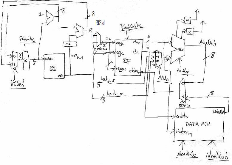
Where we also introduced a third option for the second operand of the ALU, Imm3 from the instruction and is needed for SHIFT.
All control signals are shown underlined.
We now how a complete datapath for our architecture. We thus proceed to design the CONTROL.
Designing the CONTROL
unit:
The control unit is responsible for setting all control signals of the datapath, so that all appropriate actions take place per instruction. It accepts several inputs from the datapath and produces values for the datapath’s control signals. In our architecture and for the single cycle implementation the control will be a combinatorial circuit that accepts as inputs the following signals:
INST0 through INST3 --> these are needed because these bits determine the operation of the current instruction.
N and Z --> these are needed by branch instructions to determine whether the branch is taken or not, i.e., what value should the PC be loaded with.
In turn, the control will produce the following control signals:
PCSel --> if the PC is loaded with a new value which it is going to be: 0 for PC + 1, 1 for PC + sign-extend(Imm4)
PCWrite -> 1 if we want the PC to be loaded with a new value (we will always want this)
RegWrite -> 1 if the instruction writes a register
MemRead and MemWrite -> 1 if the instruction is a load or a store respectively
R1Sel -> 1 if we
want to explicitly set K1 as the source and destination for ORI, setting this 0
passes the R1 field from the instruction opcode
(drives reg0 and regw).
ALUop -> what operation should the ALU perform (we assigned values for this signal in the description of the ADD instruction)
ALU2 -> what will drive the second input of the ALU -> 00 = second output from the register file, 01 = Imm5 field from the instruction (for ORI), 10 = Imm3 from the instruction (for SHIFT). 11 = reserved for future expansion.
RFin -> if this instruction writes a value into the register file where this value should come from: 0 = From the ALU, 1 = from the Data Memory.
Since the control unit is a combinatorial circuit we start by deriving a truth table for it:
|
INSTRUCTION |
Inputs |
Outputs |
||||||||||
|
|
INST0-3 |
N |
Z |
PCSel |
PCWrite |
RegWrite |
MemRead |
R1Sel |
MemWrite |
ALU2 |
RFin |
ALUop |
|
LOAD |
0000 |
X |
X |
0 |
1 |
1 |
1 |
0 |
0 |
X |
1 |
XXX |
|
STORE |
0010 |
X |
X |
0 |
1 |
0 |
0 |
0 |
1 |
X |
X |
XXX |
|
ADD |
0100 |
X |
X |
0 |
1 |
1 |
0 |
0 |
0 |
00 |
0 |
000 |
|
SUB |
0110 |
X |
X |
0 |
1 |
1 |
0 |
0 |
0 |
00 |
0 |
001 |
|
NAND |
1000 |
X |
X |
0 |
1 |
1 |
0 |
0 |
0 |
00 |
0 |
011 |
|
ORI |
X111 |
X |
X |
0 |
1 |
1 |
0 |
1 |
0 |
01 |
0 |
010 |
|
SHIFT |
X011 |
X |
X |
0 |
1 |
1 |
0 |
0 |
0 |
10 |
0 |
100 |
|
BZ |
0101 |
X |
0 |
0 |
1 |
0 |
0 |
X |
0 |
X |
X |
XXX |
|
|
0101 |
X |
1 |
1 |
1 |
0 |
0 |
X |
0 |
X |
X |
XXX |
|
BNZ |
1001 |
X |
0 |
1 |
1 |
0 |
0 |
X |
0 |
X |
X |
XXX |
|
|
1001 |
X |
1 |
0 |
1 |
0 |
0 |
X |
0 |
X |
X |
XXX |
|
BPZ |
1101 |
0 |
X |
1 |
1 |
0 |
0 |
X |
0 |
X |
X |
XXX |
|
|
1101 |
1 |
X |
0 |
1 |
0 |
0 |
X |
0 |
X |
X |
XXX |
Here’s the rationale behind some of the lines:
For LOAD: The INST0-3 bits should form the pattern 0000. It doesn’t matter what N and Z are since LOADS always read from memory. The PC should be changed to PC+1 thus PCSel = 0. We do change the PC thus PCWrite= 1 (turns outs that PCWrite should always be 1). We do write into the register file thus RegWrite = 1. We read from memory thus MemRead = 1. We do not write to memory thus MemWrite = 0. We do not use the ALU so, it doesn’t really matter what inputs we provide to it and what calculation it performs. Also, R1Sel = 0 as we will write into the R1 specified by the instruction opcode (and not K1 which is used only for ORI).
For NAND: The INST0-3 bits should form the pattern 1000. It doesn’t matter what N and Z are. PCSel = 0 and PCWrite = 1 since we want to simply increment the PC. MemRead and MemWrite should both be 0 since with do not read or write from/to data memory. ALU2 should be 00 since we want the second register value from the register file. RegWrite = 1 since we do write to the register file. RFin = 0 since we will write the value produced by the ALU. Finally ALUop = 011 since earlier we assumed that this is the way we ask of the ALU to perform an NAND.
For BZ: The INST0-3 bits should form the pattern 1001. It does matter what the Z flag is. So there are two lines one for when Z is zero hence we do PC = PC +1 and one for when Z = 1 in which case we do PC = PC + Sign-extend(Imm4).
Double-check all values and try to understand why they are set the way they are.
Now that we have the truth table we can implement each of the outputs of the control unit using any of the methodologies learned during digital design. Here are a few trivial implementations:
MemWrite = Inst3’ * Inst2’ * Inst1 * Inst0’
MemRead = Inst3’ * Inst2’ * Inst1’ * Inst0’
RegWrite = Inst3’*Inst2*Inst1 + Inst0’*Inst1+Inst2’*Inst1’*Inst0’+Inst3’*Inst1’*Inst0’
Timing – Putting it
all together
While we have mentioned how the timing works it is best if we revisit this issue now that everything has been put into place.
So execution of an instruction commences immediately after the falling edge of the clock.
Notice that at this point in time the signals of the datapath and the control will have values which may be incorrect (they me correct only incidentally). So, because the PC is connected to the instruction memory the latter will start reading the contents of the memory location pointed to by the PC. After a while these contents will appear on the INST lines. After a while the control will produce the appropriate control signal values In the meantime, the register file may have been reading arbitrary registers, the ALU may have been producing arbitrary results. This is OK as it does not change any storage elements (registers or memory). Eventually, once the INST signals are set correctly by the instruction memory, the register file will see the right register names on its inputs and will after a while produce the appropriate values on its outputs. Because the control will eventually produce the appropriate values for all control signals we will eventually see the appropriate results out of the ALU, or from or to memory. Key to making the whole thing work correctly is that no storage element will change prior to the next falling edge of the clock. Thus if we make the clock slow enough there will be sufficient time to produce all appropriate values and then make the right changes instantaneously.