For a comprehensive survey (including a tutorial) on circuit innovations on ferroelectric memories, please refer to the following article by Ali Sheikholeslami and P. G. Gulak: A survey of circuit innovations in Ferroelectric random-access memories, Proceedings of the IEEE, Vol. 88, No. 3, pp. 667-689, May 2000. pdf file .
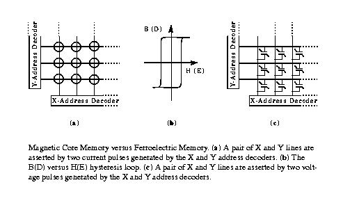
Ferroelectric capacitors possess the two characteristics required for a nonvolatile memory cell, that is they have two stable states corresponding to the two binary levels in a digital memory, and they retain their states without electrical power. Although similar characteristics exist in ferromagnetic cores of a core memory, ferroelectric capacitors switch faster and they can also be fabricated on a single VLSI chip.
The following figure compares a magnetic core array and, its counterpart, a ferroelectric capacitor array.
The capacitor array forms the simplest and the densest cell structure among ferroelectric nonvolatile memory designs. However, more complex structures are required due to nonideal characteristics of ferroelectric capacitors. One of these characteristics is the lack of a unique switching voltage. Partial switching can occur within a range of applied voltage. If this range is wide enough, the cells that are in the same row (or column) as the selected cell can be disturbed by X (or Y) voltage pulses. The effects of these partial switchings in an unselected cell can add up and totally destroy the stored information.
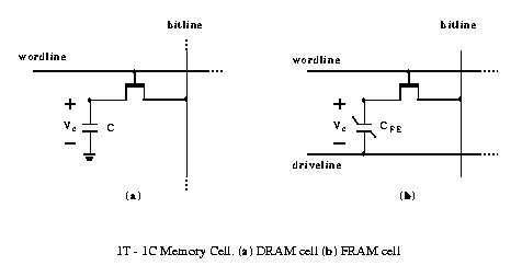
In order to write a binary digit 0 (positive polarization state) to a cell, a positive voltage (normally the full power supply voltage, VDD) is applied to the bitline while the driveline is grounded and the wordline is asserted. In writing a binary digit 1 (negative polarization state), a positive voltage (VDD) is applied to the driveline while the bitline is grounded and the wordline is asserted. Note that a negative voltage would be required on the bitline to produce the same voltage across the FE capacitor if the driveline were grounded. Also note that the equivalent circuit in the write operation is the FE capacitor in series with the access transistor ON resistance. Consequently, there is an effective time constant that limits the writing speed.
A cell can be read by floating the bitline and applying a positive voltage (VDD) to the driveline while asserting the wordline. If the initial polarization state of the capacitor is negative (positive), reading the cell develops a relatively large (small) signal on the bitline. Since this operation is destructive, the data must be written back into the cell after each read (data restore). The equivalent circuit in the read operation is the FE capacitor in series with the bitline capacitor. Therefore, the capacitance ratio of the bitline to the FE capacitor determines the available voltage for polarization switching of the FE capacitor. A ratio of 2:1 is normally suggested for 5V power supply operation. Higher ratios will provide larger voltage for the polarization switching but, at the same time, reduces the voltage available for sensing.
The design of the 1T-1C cell is constrained by the bitline capacitance and polarization parameters of the FE capacitor as well as the sensing scheme employed for reading. The bitline capacitance is calculated by the number of cells per bitline and the bitline parasitic capacitance. The polarization parameters are determined by hysteresis loop or pulse measurements.
We would appreciate
your comments and suggestions.
This page is maintained by Ali Sheikholeslami. Created on July 4, 1997. Last modified on July 19, 2000.