Next: About this document ...
Errata
for
Fundamentals of Digital Logic with VHDL Design
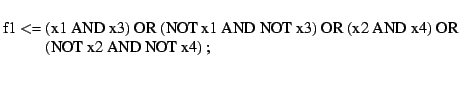
-
- Page 59
-
In problem 2.31, the equation for function f1 should be
- Page 179
-
The sixth sentence from the top of the page, which reads:
``These inversions are at inputs  ,
,  and
and  , and at the output
  .''
.''
should be changed to read
``These inversions are at inputs , , , and  and at the output .''
- Page 248
-
Near the middle of the page, the sentence that reads:
``Similarly, the expressions for  ,
,  ,
,  and
and  are''
are''
should be changed to read
``Similarly, the expressions for  and
and  are''
are''
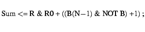
- Page 304
-
Near the end of Section 6.5 the equation
should be
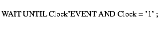
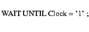
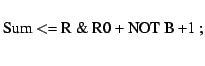
- Page 375
-
In Figure 7.41 the statement:
should be changed to remove the Clock'EVENT condition:
Please note that this problem is also present in the sample VHDL code
on the CD-ROM provided with the book.
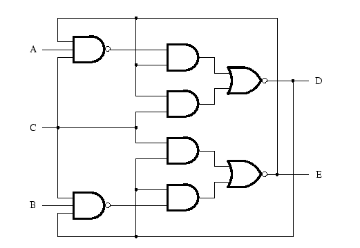
- Page 420
-
Figure P7.2 in problem 7.9 is incorrect. The intended figure is:
- Page 521
-
In Figure 9.4, the caption for part (a) should
be ``Circuit'', not ``State diagram''.
- Page 530
-
The  sentence from the bottom of the page states
``; since we are assuming that  changes first,''
This should be changed to
``assuming that  changes first in the transition from
  ,''
,''
- Page 535
-
There is an error in Example 9.6:
The circuit in Figure 9.22 is hazardous. If inputs change from r1=r2=0
to r1=r2=1, then depending on gate delays there may be glitches on g1 and g2.
The solution is to use a mutual exclusion device (ME) on the input side,
which sequences the inputs such that the arbiter circuit never sees both
inputs equal to 1.
- Page 553
-
In the middle of the page, the sentence
``Of course, this diagram can also be derived directly from Figure 9.39.''
Should be deleted. Figure 9.41 is needed for the derivation, because it shows
that D and H are not compatible.
- Page 604
-
In Figure 10.12, the caption should refer to the ``control circuit'', not the
``datapath circuit''.
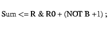
- Page 622
-
In Figure 10.28, fourth line from the bottom, the statement:
should be changed to remove the parentheses:
The parentheses cause the VHDL compiler to generate a wrong circuit, because
the number of bits in each of the two operands of the addition are not the
same. An alternative way to fix this problem is to explicitly sign-extend
the  operand:
Please note that this problem is also present in the sample VHDL code
on the CD-ROM provided with the book.
Next: About this document ...
Stephen D. Brown
2002-01-14