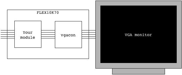
VgaCon Interface
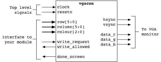
The row, column, and colour signals define the
coordinates and colour of the SuperPixel that you wish to be placed
on the screen. Set the write_request signal to '1' to write
the SuperPixel into the VGA controller memory. However,
the controller is not always able to write the pixel immediately.
It indicates this with the write_allowed signal. You must wait until
the write_allowed signal is '1' for the write to complete. When
write_allowed changes to '1' or if it is already at '1', the
SuperPixel is written on the next positive clock edge. At that point,
you can return write_request to '0'. Alternatively, you can keep write_request
at '1' to write a new SuperPixel during the next clock cycle. You can
write a new pixel every clock cycle until write_allowed is '0'.
Write
SuperPixel Timing

NOTE: With a 25 MHz clock,
it will take between 25 and 30 microseconds until write_allowed is '1'
for the first time. When write_allowed returns to '0' it will take a
similar amount of time for it to be '1' again. So when simulating with
a 25 MHz clock, be sure to set the simulation end time to at least
30 microseconds to see write_allowed change.
|
| Port/
Param |
Description |
| clock |
This
port must be connected to the clock pin in the top-level design. The
VGA controller requires that the clock pin is connected to the onboard
clock on the UP2 board for correct functionality. This can be accomplished
by assigning the clock pin to pin 91
on the FLEX10K70. |
| resetn |
The
resetn port should connect to an active low signal that forces the controller
back to its initial state. Typically this port should be connected to a
resetn pin in the top-level design. |
| row[5:0] |
These
ports should each be connected to a 6-bit signal. The signals define the
row and column coordinates of the SuperPixel that you wish to be placed
on the screen. These coordinates are automatically transformed into an
address for the memory in the controller. The column number should
be between 0 and 63, while the row number should be between 0 and 59 for the
SuperPixel to be displayed on the monitor. |
| column[5:0] |
| colour[2:0] |
This
port should be connected to a 3-bit signal which defines the colour of
the SuperPixel to be placed on the screen. Eight colours can be
produced by the Altera UP2 board. However, using all three
bits per SuperPixel consumes 66% of the dedicated memory blocks in the
FLEX10K70. If your project uses a lot of memory then you should use the
2-colour version so that less resources are consumed. The 2-colour version
uses these colours: |
| colour
= "000" |
Black
|
| colour
= "001" |
Bright Green
|
| write_request |
Set this signal to '1' to write the SuperPixel defined by
(row[5:0], column[5:0], colour[2:0]) into the controller memory.
Keep write_request set to '1' until write_allowed is '1'. At that
point, the SuperPixel is written on the next positive clock edge. Then
you can return write_request to '0'. Alternatively, you can keep write_request
at '1' to write a new SuperPixel during the next clock cycle. You can
write a new pixel every clock cycle until write_allowed is '0'. |
| write_allowed |
This signal indicates that writing pixels is currently allowed. If
write_request is set to '1', a SuperPixel will be written on the
next positive clock edge. You can write a new pixel every clock cycle
for as long as write_allowed is '1'. When write_allowed is '0' the
controller is not accepting write requests and you must wait until
write_allowed is '1' for your write to complete. |
| done_screen |
This
signal indicates that the entire screen has been drawn. The controller
asserts this signal high for one clock cycle every 16.6ms. This signal is useful
for timing and delay purposes. The demo program below uses this signal to flash
a diagonal line on the screen approximately every half-second. |
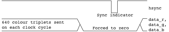
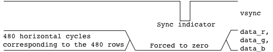
| hsync |
Produces
the horizontal and vertical sync signals for the VGA monitor. These ports must connect to top-level
output pins that must be assigned to pins 240 and 239 respectively
on the FLEX10K70. |
| vsync |
| data_r |
Produces
the red, green, and blue signals for the VGA monitor corresponding to the contents of the VGA
controller RAM. Again, these ports must connect to top-level output pins
which are assigned to pins 236, 237, and 238
respectively on the FLEX10K70. |
| data_g |
| data_b |
| ramfile |
This
is a parameter which should be assigned to a MIF file that contains
the initial contents of the controller RAM memory. It allows one to easily
create an initial picture that is displayed on the screen. A utility is
provided below which can convert standard graphic files to MIF format. |
|
VGA Demo
Instructions:
- Save the 2-colour demo or the 8-colour demo to your home directory.
- Double-click and downloaded file to create a directory that contains the files listed below.
- Open the project file (vga_demo.qpf) in Quartus.
- Compile the design.
- Download the design to the FLEX10K70 on the UP2 board. The programming switch on the board must be in the up position. The demo displays a mailbox in the background. Push the button
labelled FLEX_PB2 to turn on the flashing diagonal line.
|
| File |
Description |
| vga_demo.qpf |
The Quartus
II project file for the VGA demo. |
| vga_demo.qsf |
Contains
the PIN and DEVICE assignments for the VGA demo. |
| vgacon.vhd |
Simple
VGA controller written in VHDL. |
| vga_demo.v |
A
Verilog file which demonstrates the use of VgaCon. |
| vga_demo.mif |
Initial
RAM contents for the VGA controller. This contains the picture of the mailbox
that is displayed initially by the demo. |
| pbmtomif.c |
Converts
a graphics file in PBM (ASCII) format to a MIF file that can be loaded into the
VGA controller RAM memory. This program was used to convert a PBM graphic
of the mailbox into the demo MIF file. It is particularly useful if you
wish to create an initial background for applications such as tic-tac-toe
game. You can draw the background with any graphic editor, shrink it to
a 64x64 resolution and save it in PBM format. xv is a graphical UNIX program that
will allow one to convert common graphic formats such as GIF, JPEG, and
BMP to PBM. Instructions for compiling and running PBMtoMIF are in this source file. |
|
Creating Your Own Project
You need to download projects that involve VgaCon into the FLEX10K70
on the UP2 board. Pin locations for this device can be found
in the Altera
UP2 User Guide.
|