Table of Contents
The video-in controller provides a simple interface to the video decoder chip present on the DE2 board. The video decoder chip, as connected on the DE2 board, accepts the composite video input through the Video-In jack on the DE2 board. The controller handles the data transmission and processing which is necessary to obtain the picture data in a simple format. The chip configuration is handled by the separate configuration module, which must be instantiated when using the video-in controller.
This document will describe the interface and operation of the video-in controller.
You can download the source code (in Verilog) for the video-in controller here. Please note that this code works with the first revision of the DE2 board. If you experience problems, it is likely that you have a second revision of the board, and the small change is required, as described in the section called “Changes for the newer revision of the DE2”.
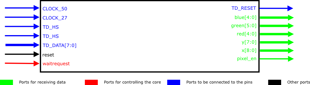
The video-in controller interface is illustrated in Figure 1, “Video-in controller”, with inputs shown on the left, outputs and bidirectional lines on the right. Ports are used as follows:
CLOCK_50- system clock input, must be 50MHz for the timing control to work properly.reset- the active-high reset.CLOCK_27,TD_DATA,TD_HS,TD_VS,TD_RESET,I2C_SDATandI2C_SCLK- off-chip lines to be connected to the correspondingly named pins, as defined in this file.
Ports for receiving data
xandy- Coordinates for the current pixel.red,greenandblue- RGB color values for the current pixel, 16 bits in total.pixel_en- indicates that the coordinate and color signals are valid. This signal is synchronized to the 50MHz clock (CLOCK_50) and acts as an enable signal.
Ports for controlling the core
waitrequest- if this signal is asserted, the audio controller will wait until the signal is deasserted again before sending any more data. Please note that the data is buffered while the signal is asserted, and the buffer capacity is limited. It is safe to assign this signal a constant zero if the data buffering will not be necessary for the user application.
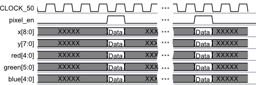
The video-in controller interface is analogous to the interface used by the VGA adapter, except the data is received instead of sent.
The X and Y coordinate outputs set the location of the current pixel, and the RGB color outputs set
the pixel color. The pixel value should be captured on the positive edge when the pixel_en
signal is high. Each frame (video is composed of a series of images called frames) has a resolution of
320x240, and the color depth is 16 bits per pixel.
The interface is illustrated in Figure 2, “Interface timing diagram”.
The sample circuit using the video-in controller is available here. You are provided with the full Quartus project and the .sof file already compiled and ready to be programmed. The project contains all the assignments necessary for the proper operation of the circuit, and it is recommended to start with this sample project if you wish to use the video-in controller in your design. If you do not start with this sample project, you must either import the project settings, or make the necessary assigments manually, as described in the section called “Important implementation notes”.
The circuit in this sample project simply connects the video-in controller to the VGA adapter. If you connect the video source to the Video-In jack on the DE2 board, you should see the same video on the VGA monitor. Please note that the video will be of a very low quality, because the VGA adapter is only capable of displaying 8 colors at a low resolution.
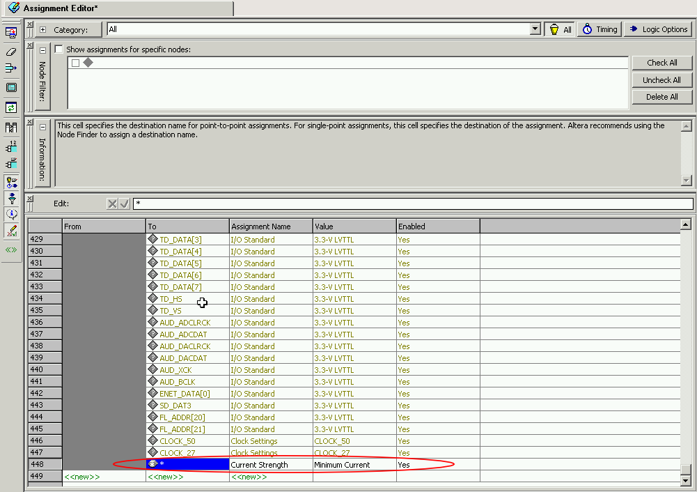
Note that in order for the video-in controller to function properly, you must change some of the pin characteristics. The FPGA pins are not just metal pins that connect to the outside world, but are configurable. This allows the FPGA to connect to a wide range of other devices. The change is only necessary if you start a new project, because the sample project already contains the required assignments.
To make the required assignments, open the Quartus project, go to the Assignments menu, select the Assignment Editor, scroll down to the bottom of the list and create a new entry called Current Strength. Set it to Minimum Current, and assign the setting to all the pins by putting the '*' (asterisk) as the pin name (To field). The resulting entry is shown in Figure 3, “Screenshot of the Assignment Editor”. The asterisk implies that you are setting all of the pins. For your purposes, you do not need to understand what the setting Minimum Current is.
In case you need a higher current for other pins, you can create more assignments and set the current as required.
The newer revision of DE2 board has a slightly different pin connections, and as a result, a small change is required in order for the video-in core to function properly.
The problem manifests as the jittering and distortion of the image when running the video-in demo. If you experience these effects, it is most likely that you have a new revision of the DE2 board, and the modification described below is recommended. You can also find out the revision of your board by checking the serial number. The serial numbers of the newer revision boards start with 1, while the old ones start with 0. The serial number can usually be found on the bottom of the DE2 board.
The simplest way to resolve the problem is to reassign the pin CLOCK_27 to the
location PIN_C16. You can do so either using the pin editor (launched from the
Assignments menu), or using the Assignment Editor as described
above.
This section describes the operation of the video-in controller in more detail, and is only relevant to those who wish to modify the controller or learn about its operation. The understanding of this material is not required for the usage of the video-in controller.
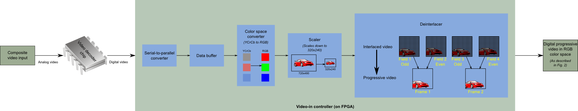
The video-in controller performs a series of data processing operations to simplify the data format. The signal path is illustrated in Figure 4, “Video signal path”.
The data received from the video decoder is first converted to the RGB color space. Color space describes a way to encode the color information, and the conversion is necessary because the original video is encoded in the YUV color space, which is unsuitable for display on the VGA monitor.
Then the frames are scaled down from the 720x480 to the 320x240 resolution to simplify the interfacing with the VGA adapter.
Finally the deinterlacing is performed to recover the progressive video. The video from the standard NTSC sources is interlaced, which means that every frame only has either the odd or the even lines. This would be very inconvenient to use with the digital displays, so the deinterlacing is performed, and the progressive video is recovered.
Progressive video is just a series of frames, and can be displayed directly using the VGA adapter.
If you wish to learn more about interlaced and progressive video, why the deinterlacing is needed, and more, the good places to start are Wikipedia and this FAQ on deinterlacing.