ECE1388: VLSI Design Methodology
Final Project
256kbit SDRAM Design
Rebecca Au & Keith Tang
Introduction
In this project, a 256k synchronous DRAM is designed in 0.35-mm CMOS technology. It consists 4 memory banks; each has a size of 256 x 256 bits. The DRAM is referenced by column address in each 16-bit word. During Read/write operations, the 16-bit word is read or written to the output buffer in parallel. It has a total of 32 I/O pins: 8 for row/column address, 2 for bank address, 16 for data input/output, 3 for power and ground, 3 others for row/column address select and refresh. It supports Read/Write, Burst, and Refresh operations. All commands and operations are executed on the falling edge of the master clock signal, CLK. The DRAM operates with a clock frequency of 50 MHz. The core area is 1950 mm x 1750 mm, with the memory bank taking 76 % of the area. Total area with I/O pad is 2362 mm x 2070 mm.
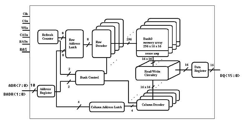
The block diagram is shown in Fig. 1.
Fig. 1 SDRAM Block Diagram
Operations
Read/Write
The WriteEn signal selects either Read or Write operation: WriteEn HIGH for write and LOW for read. The data is read or written to the memory locations in 2 clock cycles. In the first cycle, the row address is latched into the decoder on RASn LOW. In the next cycle, the column address is latched into the decoder on CASn low. At the next falling edge of CLKn, the address is decoded, the memory cells are sensed by sense amplifier and the data is read from or is written to the output buffers. As shown in Fig. 2, the delay between falling edge of the CLKn and the rising edge of the selected word line is 3.8 ns. The large delay is required because it takes some longer delay for the ripple counter to generate address incrementally during refresh or burst operation. The delay from the falling edge of the CLKn and the rising edge of the selected column line is 4.5 ns. The delay to the column select line must be longer than that to the word line, as selected bitline is turned on after the wordline.
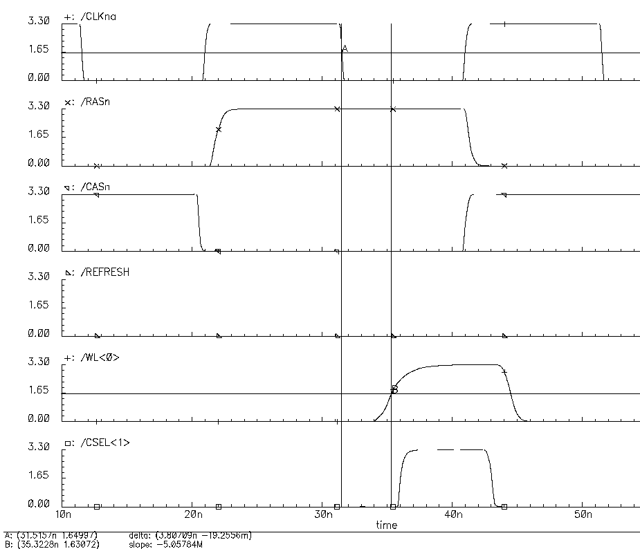
Fig. 2 Simulation Result showing the delay from CLK to selected wordline and column
Refresh
The dynamic nature of DRAM requires that the memory be
refreshed periodically so as not to lose the contents of the memory cells.
It is accomplished internally by the refresh counter in the row address
buffer. In refresh mode, the memory
is accessed with every possible row address combination.
The refresh operation requires 10.24
mm
to refresh all memory locations. The
memory cells should be refreshed every 28 ms. Therefore, the DRAM is unavailable
about 0.036 % of the time for refresh. The
Refresh mode is selected by putting REFRESH HIGH.
Burst
The burst mode can be used to access each word incrementally in the selected column. In the Read/Write operation, the desired memory location is accessed. Then, in burst mode, the word line is incremented and the data of the selected column is read/wrote word after word.
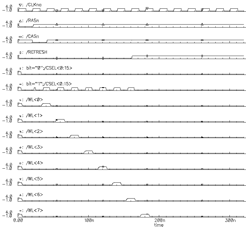
Fig. 3 Simulation result showing wordline selected incrementally in burst and refresh Operation
Blocks in the SDRAM
Memory Cells and Banks
The memory cell comprises two NMOS transistors, as shown in
Fig. 4. One of the NMOS transistors
is connected from source to drain, and the pn-junction acts as a planar storage
capacitor. The gate of the other
transistor is controlled by the wordline for accessing the storage capacitor.
The drain and source of the storage transistor are shared to minimize
layout area. It is also shielded by
a ground line to minimize signal coupling.
Considering the wordline is connected to the gate of the memory cells, it presents a large parasistic load on the wordline and degrades the circuit speed. So the memory is split into 4 banks at the cost of a larger layout area. Each bank consists of 256 x 256 bits, as shown in Fig. 5. A folded bitlline structure is used to minimize noise. The wordline is layout using polysilicon, which allows the NMOS to be formed by crossing the poly wordline over an n+ active area. In order to minimize the parasitics on the wordline, Metal 3 is connected in parallel with the polysilicon, with contacts in every 16 cells.
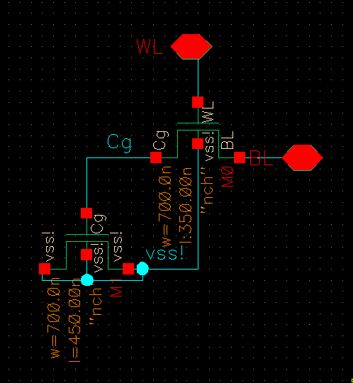
Fig. 4a Schematic of Memory Cell
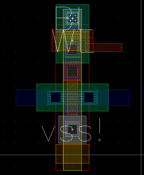
Fig. 4b Layout of Memory Cell
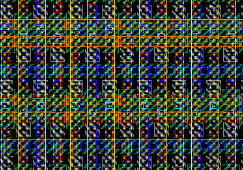
Fig. 5 Layout of Memory Bank
Sense Amplifier
Each sense amplifier is shared by the top and bottom memory arrays. The sense amplifier consists of equilibration and bias circuits, isolation devices, input/output transistors, Nsense- and Psense-amplifiers, as shown in Fig. 6. During precharge, the bitline is precharged to Vcc/2 by the equilibration and bias circuits. Then, in active mode, the isolation devices isolate the non-selected array. When the column line is selected HIGH, the sense amplifier pulls the bitlines HIGH or LOW depending on the stored charge. The simulation plot is shown in Fig. 7.
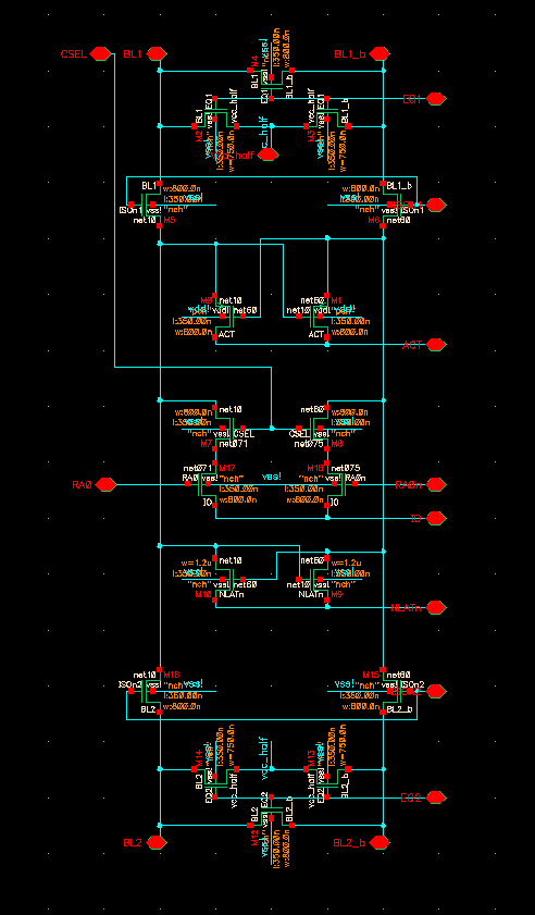
Fig. 6a Schematic of Sense Amplifier
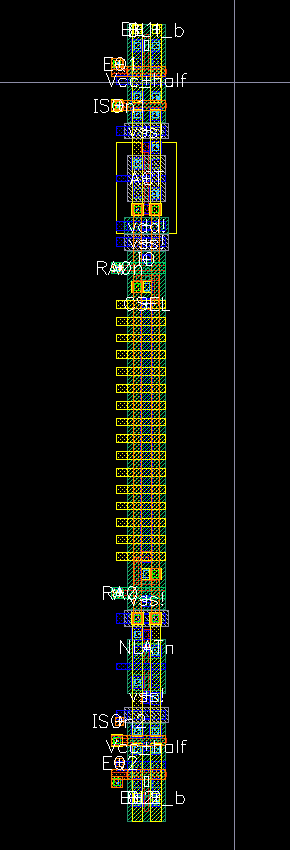
Fig. 6b Layout of Sense Amplifier
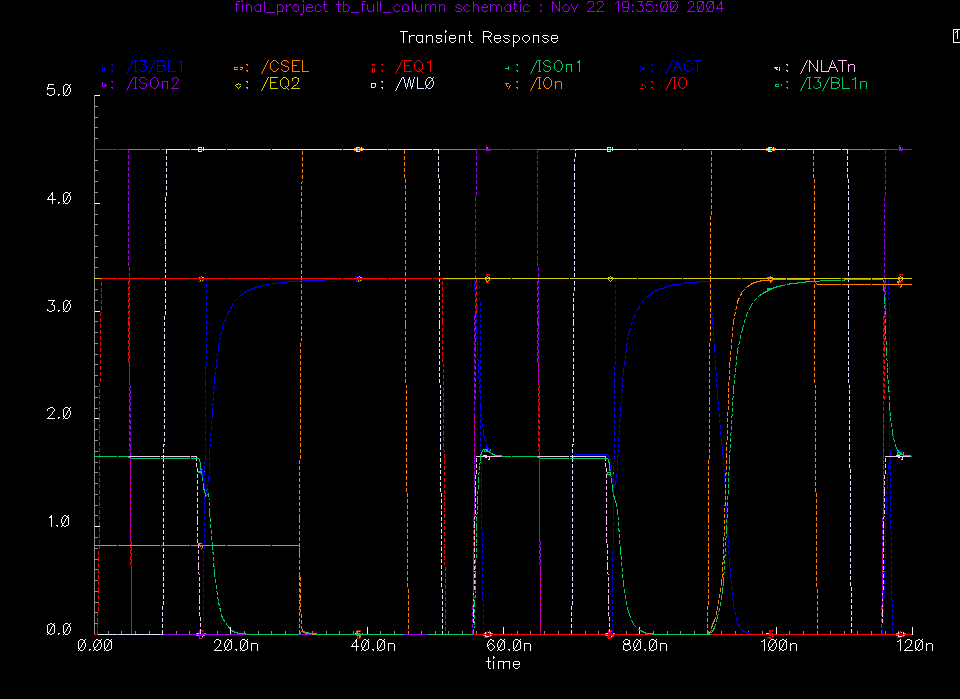
Fig. 7 Simulation Plot of Sense Amplifier
Decoders
Row/Column decoder is used for decoding the input address
bit for accessing one of the wordlines/bitlines. Dynamic logic is used to increase speed, lower power and
minimize layout area.
The 8-to-256 bits row decoder is designed to access one of
the 256 word lines in the memory bank, as shown in Fig. 8,
The row decoder consists of 6 stages of NAND-INV-NAND-INV-NAND-INV cells.
Predecoding is used for the advantages of lower power, higher efficiency
and simplified layout. The 8-bit
row address is first predecode into 16 bits using NAND-INV.
The 16-bit is further predeocde into 32 bits using NAND-INV.
In the last stage, the predecoded logic is passed to the NAND-INV and
decode to 256 bits for accessing one of the 256 wordlines.
Similarly, the 4-to-16 bits column decoder is designed to
access one of the 16 column lines (each column line access a 16-bit word), as
shown in Fig. 9. It consists of 4
stages of NAND-INV-NAND-INV. The
4-bit address is predecoded to 8-bit, which is then decoded to 16-bit in the
last stage.
The bank decoder is used to select one of the 4 memory banks. It consists of simple NAND-INV-INV-INV cells, as shown in Fig. 10.
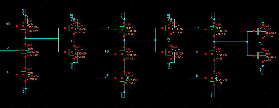
Fig. 8a Schematic of 1 path of the 6 Stages Row Decoder
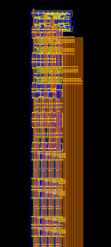
Fig. 8b Layout of Row Decoder
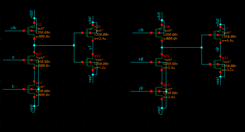
Fig. 9a Schematic of 1 path of the 4 Stages Column Decoder
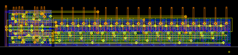
Fig. 9 Layout of Column Decoder
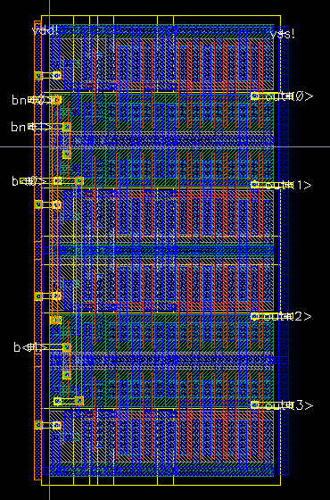
Fig. 10 Layout of Bank Decoder
Row/Column Address Buffers
The address buffer consists of input inverter, latch and refresh circuitry (for row address buffer only), as shown in Fig. 11. The input inverter drives through a mux, which is controlled by clock. When the clock is low, the mux is enabled. The refresh counter consists of a single inverter and a pair of inverter latches coupled through a pair of complementary muxes to form a one-bit counter. For every HIGH-to-LOW transition of CLK, the register output toggles. All of the one-bit counters are cascaded together to form a ripple counter. The latch, consists of two inverters and two input muxes latches the row address after RAS falls. The feedback inverter has low drive capability, which allows the latch to be overwritten by either the address input buffer or the refresh counter.
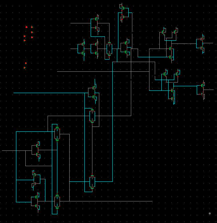
Fig. 11a Schematic of Row Address Buffer
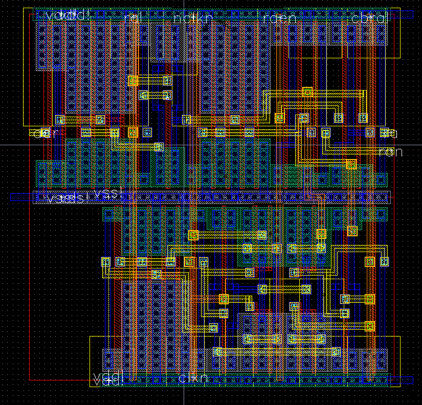
Fig. 11b Layout of Row Address Buffer
Full Chip Layout
The full chip floorplan of the core area is shown in Fig. 12 and layout is shown in Fig. 13. Total area of the core is 1950 mm x 1750 mm and 2362 mm x 2070 mm with I/O pads. The 4 memory banks, which take up 76 % of the total core area, are placed slightly off-center with spaces to the left for row decoder and row address buffers. The sense amplifiers are placed in middle between two memory banks. Space is left between the row decoder and the memory banks for routing 256 x 2 wordline signals to the memory elements. The column detector and column address buffers are relatively small in area and is placed at the bottom of the row detector and next to the sense amplifier. The I/O pins are placed near the edge of the core and can be easily routed to the I/O pads. The pad frame is shown in Fig. 14.
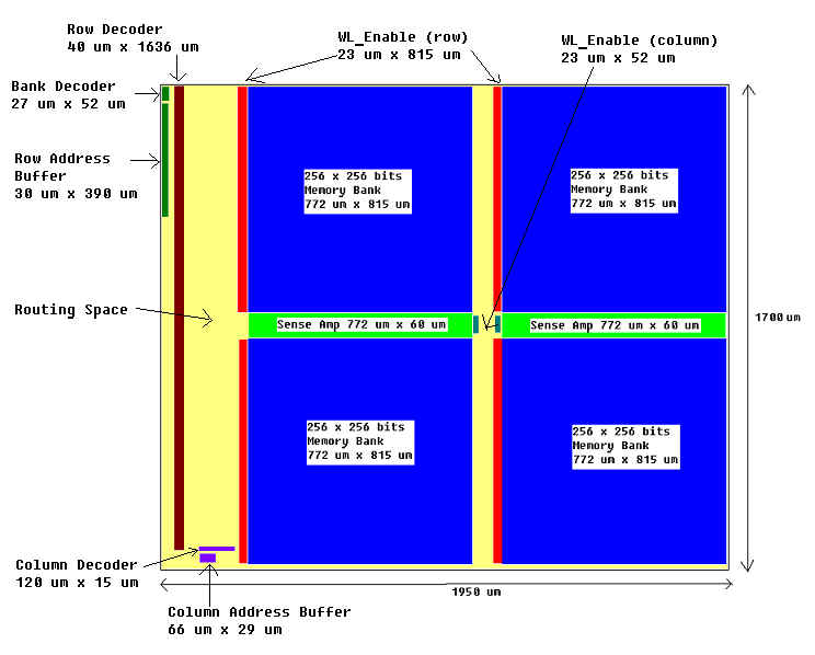
Fig. 12 Full Chip Floorplan
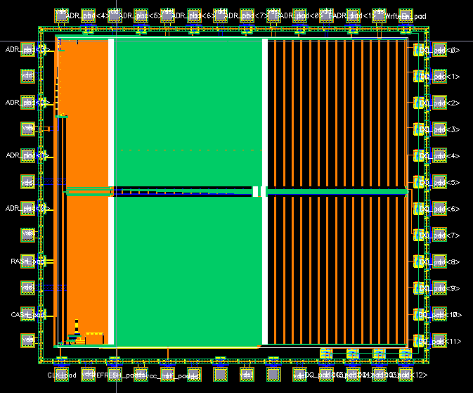
Fig. 13 Full Chip Layout
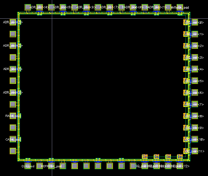
Fig. 14 Pad Frame Layout