ECE1388F – VLSI Design Methodology
Final Project:
Cache Chip Design
Jennifer Pham
Cintia Man
Shahriar Shahramian
Oleksiy Tyshchenko
January 31, 2005
1.
Introduction
This document focuses on the design of a synchronous write
through cache memory which implements least recently used (LRU) algorithm for
efficient data access. In the LRU
algorithm, the content of the least recently used cell is being replaced
whenever a write cycle is executed. The
content of the most recently used cell remains untouched in the cache. The cache chip consists of address and data
path. The address path is responsible for mapping the global memory address
(typically from external DRAM) to the physical location of data in the cache.
The data path returns the content of the physical memory location to the
requesting device (typically from a processor or controller). The address path is implemented as
2.
System
Functionality
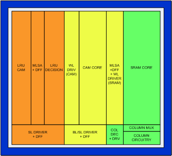
Figure 2.1
illustrates the overall block diagrams of the cache chip. The processor is
assumed to have an address space of 16 bits. The address bits (15:0) are
latched with Flip Flops before they are sent to the
·
·
SRAM:
256 Rows x 4 Blocks x 32 Bits
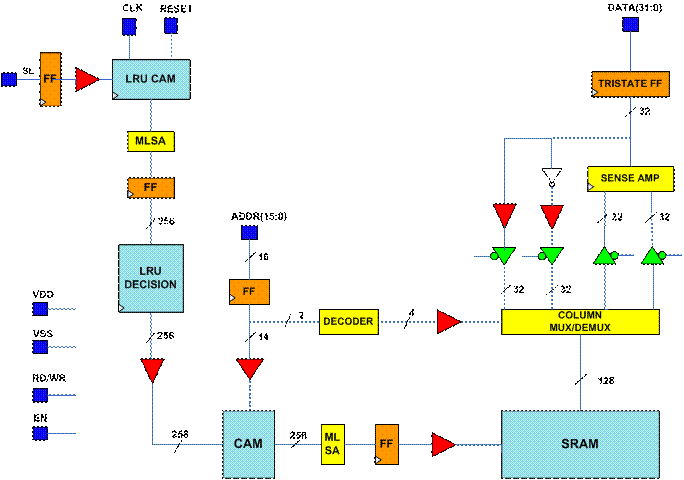
Figure 2.1: System
Block Diagram
When it comes to
replacing an element in the Cache, an LRU algorithm has been employed. A custom
LRU CAM block has been designed for which its
The over all
algorithmic description of the behavior of our Cache chip during READ/WRITE
cycles is as follows:
READ – HIT
1.
2.
The
least 2 significant bits of the address are used to select the appropriate SRAM
block.
3.
The
data is read from SRAM and sent back to the processor.
4.
The
corresponding LRU CAM ROW COUNTER is reset to “00000”.
READ – MISS
1.
2.
The
processor is notified and the LRU CAM is searched with patters to find the LRU
element.
3.
In
the meanwhile 4 words of data corresponding to the 14 most significant bits of
the address are brought from main memory.
4.
The
data from the main memory is also sent to the processor.
5.
LRU
DECISION block selects the LRU CAM row and the new address is written in the
row while 4 new words are stored in the SRAM in the same row number.
6.
The
corresponding LRU CAM ROW COUNTER is reset to “00000”.
WRITE – HIT
1.
2.
The
least 2 significant bits of the address are used to select the appropriate SRAM
block.
3.
The
new data coming from the processor is updates in the SRAM.
4.
In
the meanwhile, the data in the main memory is also updates. This is necessary
as the Cache is a write through Cache.
5.
The
corresponding LRU CAM ROW COUNTER is reset to “00000”.
WRITE – MISS
1.
2.
The
processor is notified and the LRU CAM is searched with patters to find the LRU
element.
3.
In
the meanwhile 4 words of data corresponding to the 14 most significant bits of
the address are updated and brought from main memory.
4.
LRU
DECISION block selects the LRU CAM row and the new address is written in the
row while 4 new words are stored in the SRAM in the same row number.
5.
The
corresponding LRU CAM ROW COUNTER is reset to “00000”.
In terms of
division of tasks, here is an estimate:
·
LRU
Block Circuitry: Shahriar
·
·
SRAM
Column Circuitry: Jen
·
Peripheral
Circuitry for LRU,
·
System
Integration: All team members
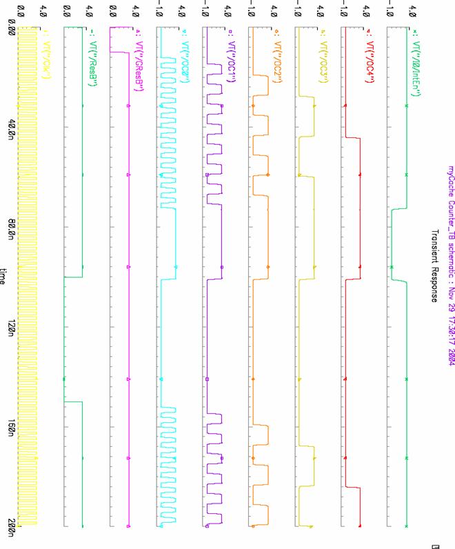
3. LRU Design
a) Circuit Schematic
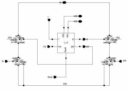
Figure 3.1:
LRU
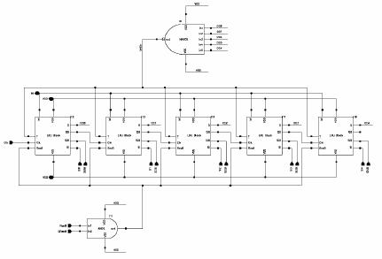
Figure 3.2:
LRU
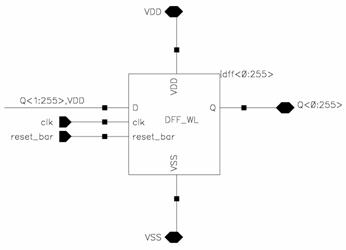
Figure 3.3:
LRU
Decision Block Schematic
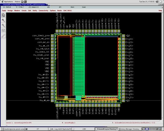
b) Cell Layout
Figure 3.4:
LRU
Figure 3.5:
LRU
Decision Block Layout
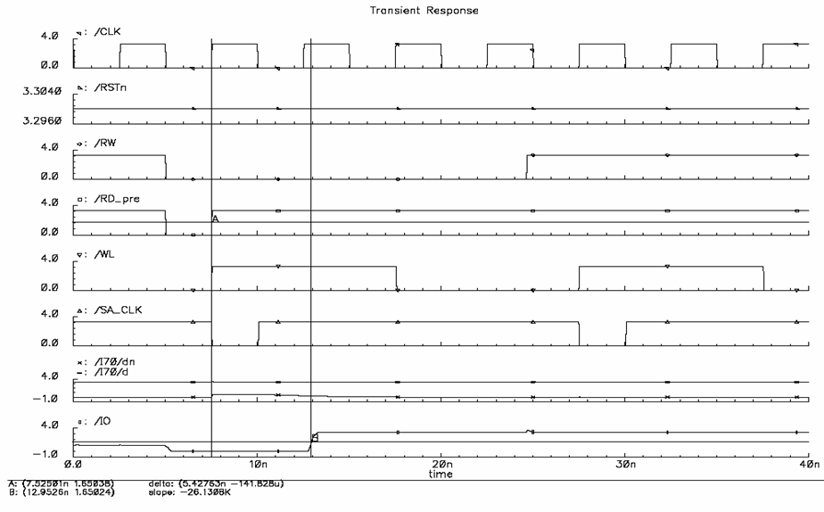
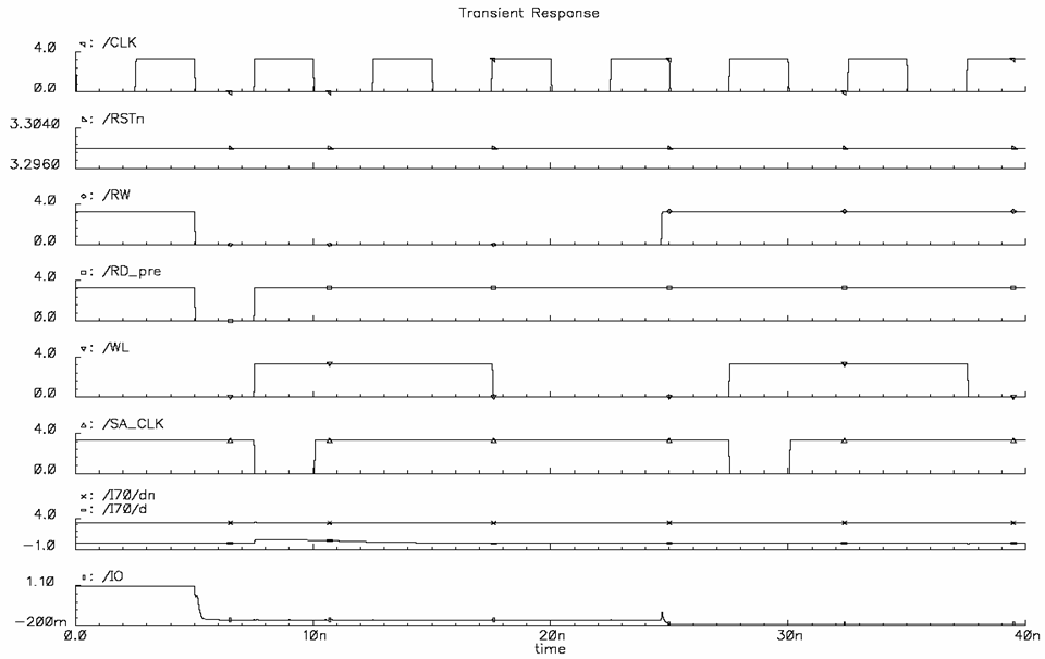
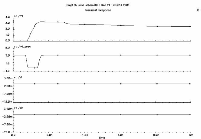
c) Simulation Results
4.
CAM
Design
a) Circuit Schematic
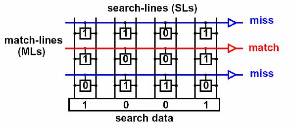
Figure 4.1:
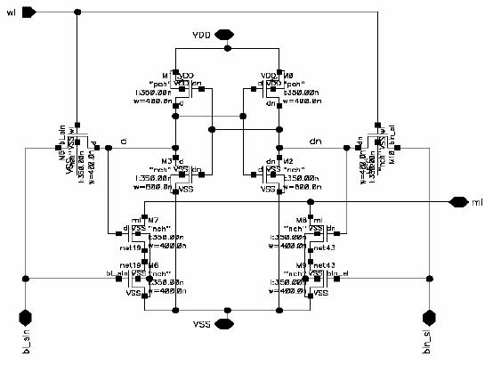
Figure 4.2:
Figure 4.3:
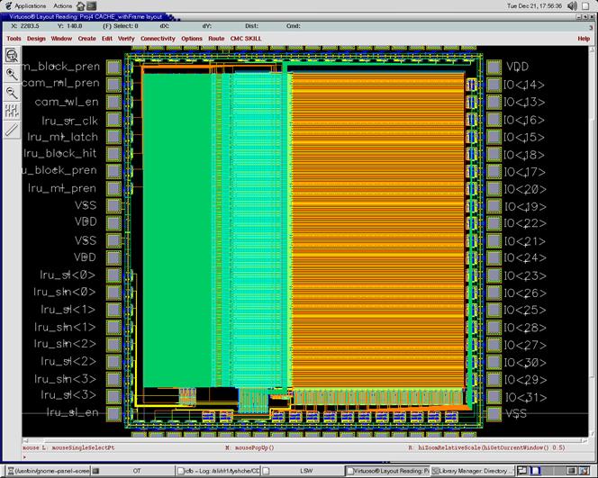
b) Cell Layout
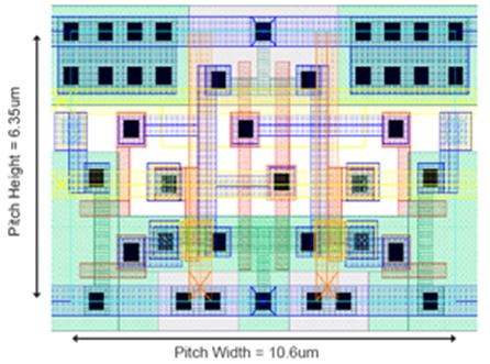
Figure 4.4:
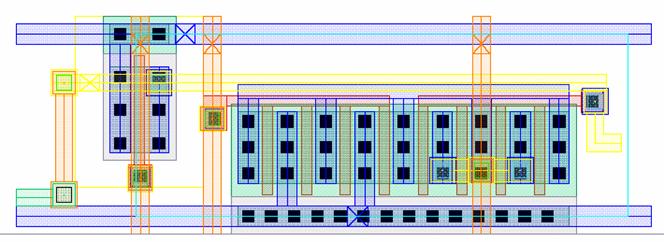
Figure 4.5:
MLSA
Layout
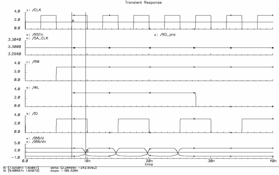
c) Simulation Results
5.
SRAM Design
a) Circuit Schematic
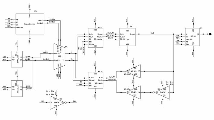
Figure 5.1:
SRAM
Column Circuitry
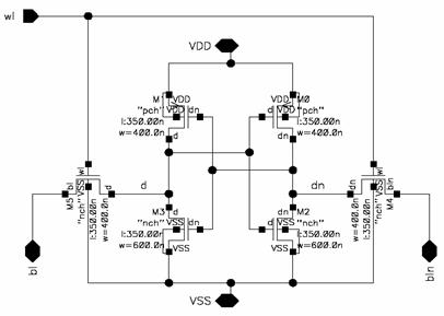
Figure 5.2:
SRAM
6T Cell
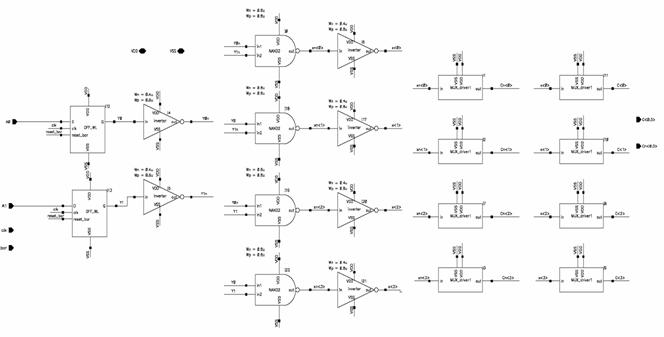
Figure 5.3:
Column
Decoder
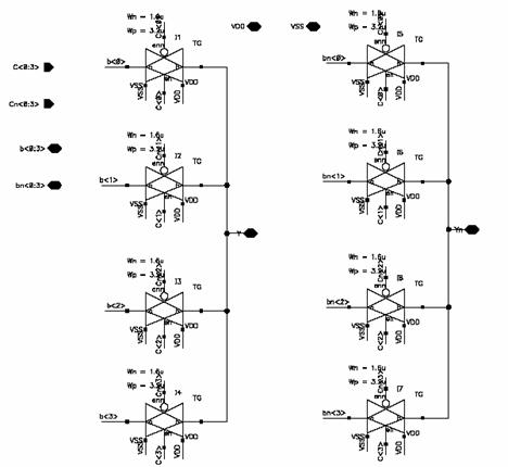
Figure 5.1:
Column
Multiplexer
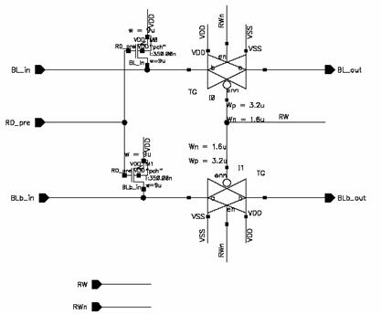
Figure 5.2:
Read
Tri-state Circuitry
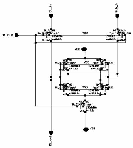
Figure 5.3:
SRAM
Sense Amplifier (SA)
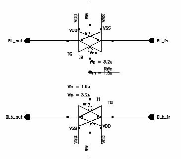
Figure 5.4:
Write
Tri-state Circuitry
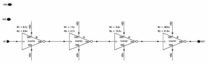
Figure 5.5:
Write
Bit-line Driver
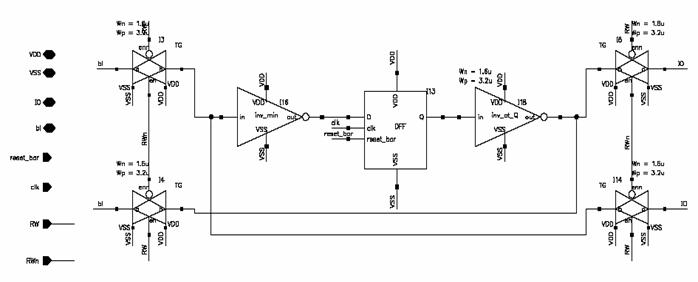
Figure 5.6:
Input/Output
Flip Flop
a)
Cell
Layout
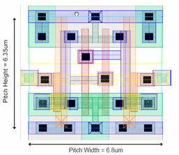
Figure 5.7:
SRAM
Cell Layout
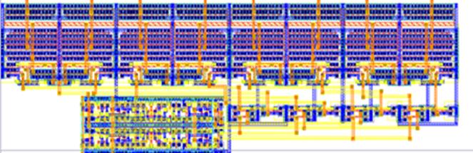
Figure 5.8:
Column
Decoder Layout
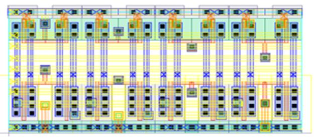
Figure 5.9:
Column
Multiplexer Layout
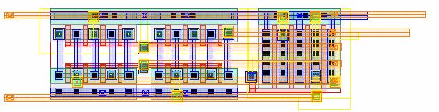
Figure 5.10:
Read
Tri-state Layout
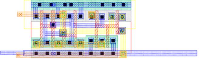
Figure 5.11:
SRAM
Sense Amplifier Layout
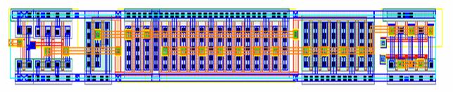
Figure 5.12:
Write
Tri-state and Bit-line Driver Layout
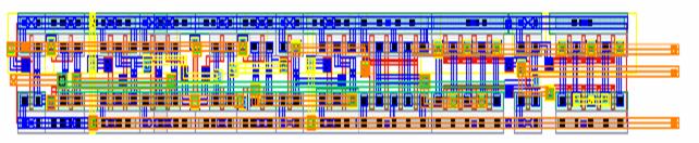
Figure 5.13:
Input/Output
Flip Flop Layout