1. Introduction
A clock-and-data recovery (CDR) circuit is used to both recover the clock from a transmitted data stream and re-time that data with the recovered clock. Such circuits are typically placed at the front-end of receiver chips to recover the clock from data sent from a transmitter chip across a backplane or other channel.
This project presents a fully-analog CDR that uses phase interpolation to adjust the phase of a locally generated 5GHz clock to align with the phase of an incoming 5Gb/s data stream.
2. System Outline
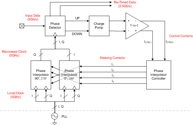
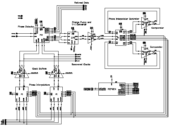
A binary phase detector performs two functions: (1) re-times the incoming data stream with the recovered clock; (2) compares the phase of the data and recovered clock, generating differential up and down pulses. These pulses are converted to DC values by a differential charge pump and loop filter. A voltage-to-current converter converts these voltages to differential currents that fed to a phase interpolator (PI) controller.
The PI controller determines the smaller of the two currents using a comparator and generates four steering currents. These currents are fed to two phase interpolators and control the degree of interpolation applied to the four-phase (i.e., differential in-phase and quadrature) locally-generated 5GHz clock. These phase-adjusted clocks are then buffered and fed back to the phase detector as the 5GHz recovered clocks, thereby completing the feedback loop. A block diagram of the CDR is shown in Fig. 1.
3. Design Advantages
- By adjusting only the local clock's phase (and not its frequency), all data channels in a receiver can share a single PLL, thus significantly reducing area and power consumption.
- Analog phase interpolator controller allows increased phase adjustment resolution and higher operating speed than digital implementations.
- Analog-only design eliminates the need to further deserialize the data for digital logic.
- Use of standard CMOS allows higher integration and less power consumption than other exotic technologies typically used for high-speed front-ends.
4. Cell Schematics
4.1 Phase Detector
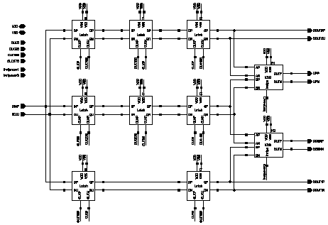
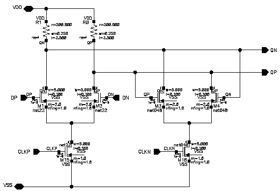
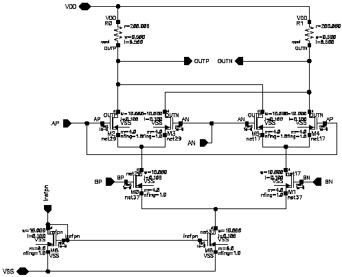
The phase detector, shown in Fig. 2 samples the data using three parallel master-slave flip-flops constructed with current-mode logic (CML) latches, one of which is shown in Fig. 3. The top path samples the data on the rising edge of the in-phase clock, the middle on the rising edge of quadrature clock, and the bottom on the falling edge of the in-phase clock. The third latch in the top two paths synchronizes all paths to the same clock edge. The two CML XORs, one of which is shown in Fig. 4, detect the phase difference between the sampled data and generate differential up and down pulses.
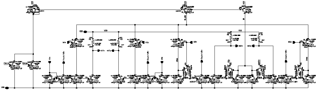
4.2 Phase Interpolator Controller
The phase interpolator (PI) controller, shown in Fig. 5, takes as input the two control currents generated by the V-I converter, I1 and I2. These currents are mirrored multiple times to (1) be output directly as steering currents for the two phase interpolators (PIs); (2) be compared by comparing the voltage drop developed across two identical resistors; (3) be summed to generate the other two steering currents, I3 and I4. The control bits b1p, b1n, b2p and b2n are digital control bits generated by two comparators.
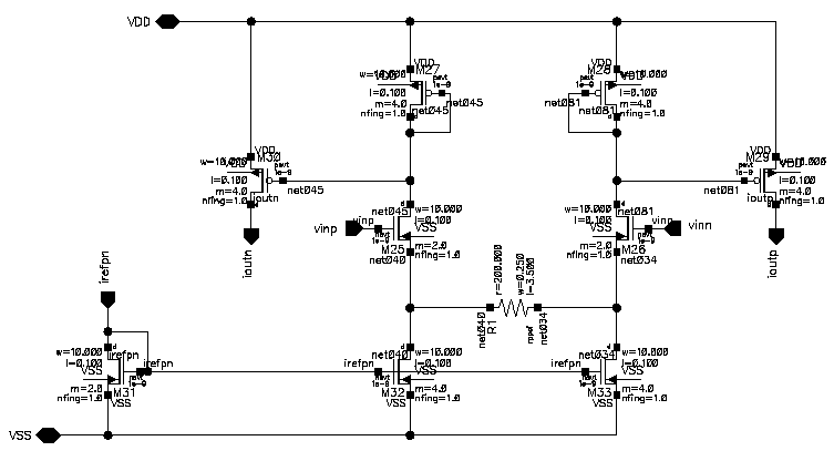
4.3 Comparator
Two comparators determine the larger of the two PI controller current pairs. The first compares the drop developed across two resistors by I1 and I2, while the other compares the drops developed by I3 and I4. The differential comparator outputs are fed back to the PI controller as the digital control bits described above. The comparator schematic is shown in Fig. 6.
4.4 Phase Interpolator
Two PIs interpolate the phase of the local four-phase clock and generate the recovered four-phase clock. The degree of interpolation depends upon the magnitude of the four steering currents generated by the PI Controller, which obey the following relationship: I1 + I2 = I3 + I4. Each PI consists of four resistively-loaded differential pairs whose currents are steered to two nodes by the local clock. One PI generates the in-phase clock while the other generates the quadrature clock by switching the order of the input currents. The PI schematic is shown in Fig. 7.
4.5 Other Schematics
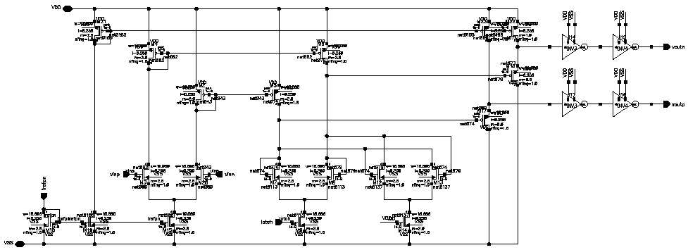
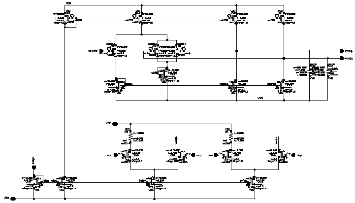
- Fig. 8. Charge pump: Converts the up and down pulses generated by the phase detector to DC values.
- Fig. 9. V-I converter: Converts the charge pump output to proportional differential currents.
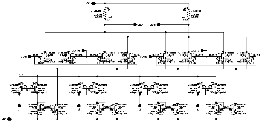
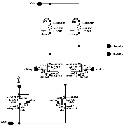
- Fig. 10. Clock buffers: Buffer the phase-interpolated clocks, generating the recovered clocks.
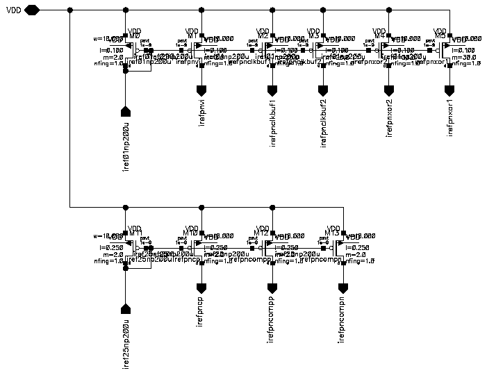
- Fig. 11. Reference generator: Generate bias currents for all blocks.
4.6 CDR Top-Level
The top-level schematic is shown in Fig. 12.
5. Simulation Results
| Technology | STM 90nm CMOS |
| Supply voltage | 1.2V |
| Data rate | 5Gb/s |
| Clock rate | 5GHz |
| Data output swing | 0.6Vpp-se |
| Clock output swing | 0.4Vpp-se |
| Power consumption | 72mW |
| Re-timed data eye opening | 0.55V |
| Recovered clock eye opening | 0.35V |
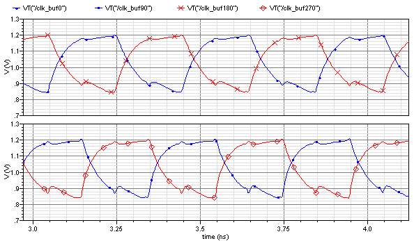
5.1 Recovered Clock
Fig. 13 shows the 5GHz recovered four-phase clock, where the top plot shows the in-phase clock and the bottom the quadrature clock.
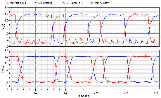
5.2 Re-timed Data
The top plot in Fig. 14 shows the 5Gb/s input data and the bottom shows the 5Gb/s re-timed data. The input data was generated with a PRBS of length 27-1.
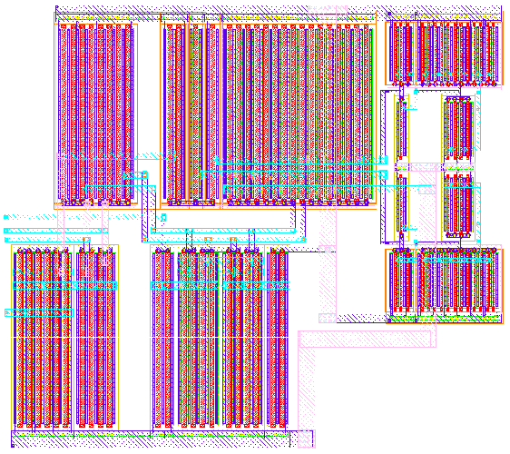
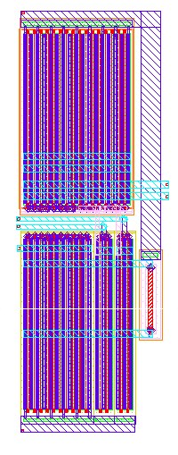
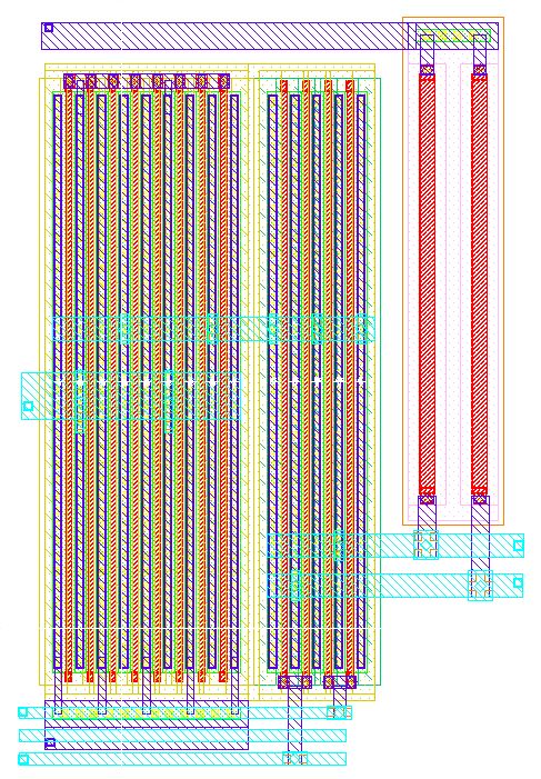
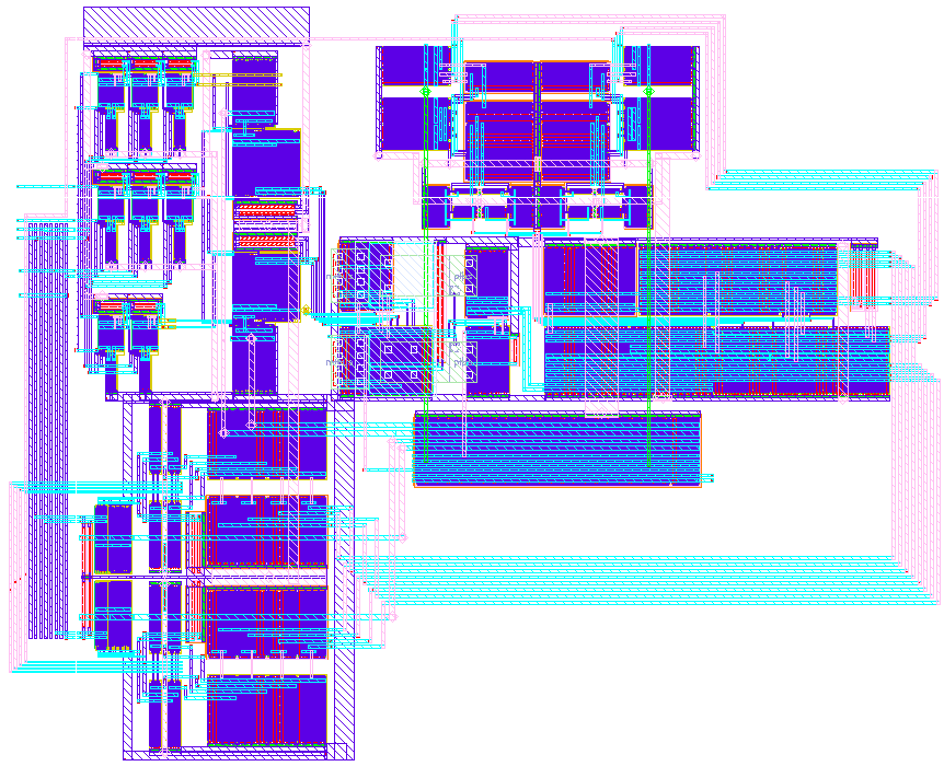
6. Cell Layouts
- Fig. 15. Phase detector
- Fig. 16. Latch
- Fig. 17. XOR
- Fig. 18. Phase interpolator controller
- Fig. 19. Comparator
- Fig. 20. Phase interpolator
- Fig. 21. Charge pump
- Fig. 22. V-I converter
- Fig. 23. Clock buffer
- Fig. 24. Reference generator
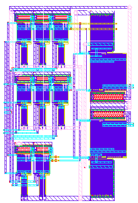
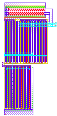
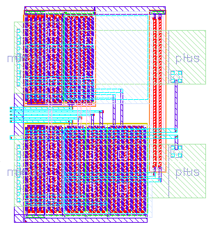
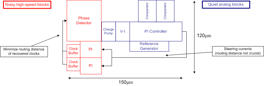
7. CDR Floorplan
The CDR floorplan is shown below in Fig. 25. The noisy high-speed blocks are powered by a separate VDD supply than the quiet blocks and hence were grouped together. The feedback nature of the CDR prevented a linear signal flow and thus dictated that some signals be routed a long distance back to the phase detector. Because the steering currents generated by the PI controller vary only when phase changes are detected in the incoming data, they are largely DC currents and therefore were chosen to be routed over this distance. This also maintained separation of noisy and quiet blocks.
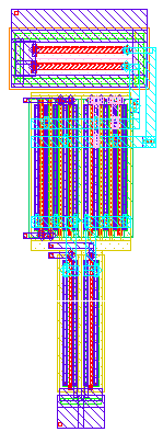
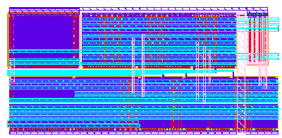
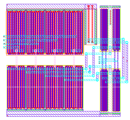
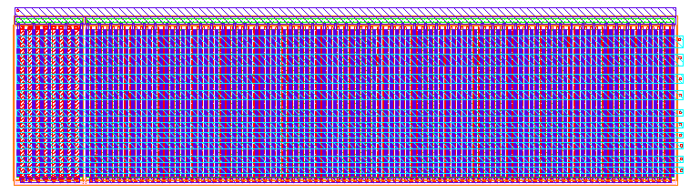
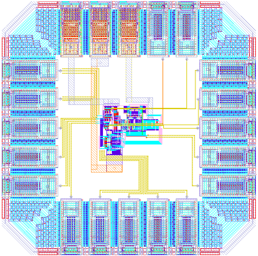
8. Chip Layout
The core, shown in Fig. 26, measures 144μm by 120μm, occupying 17,300μm2, while the padframe measures 580μm by 580μm, occupying 0.34mm2. The chip, shown in Fig. 27, contains 17 analog unbuffered I/O pads, two VDD pads and one VSS pad. The design is pad-limited, but CDRs are not developed as stand-alone products. The noisy high-speed blocks are powered by a separate VDD supply than the quiet blocks.
The two VDD supplies were separated by inserting two cuts into the padframe's VDD ring. They were routed to the circuit on the top-most layer, metal 7, while VSS was routed on metal 6. Signals were routed to the pads on metal 5 to minimize substrate coupling. Groups of input data and clocks were each first routed from the pads to a central point and then to the circuit to minimize skew.
9. LVS Report and Device Count
The LVS report for the CDR chip indicates the design is LVS clean. The total device count from all reports after tool reductions, excluding the padframe, is 388 devices.
Appendix - Diagrams, Waveforms, Schematics and Layouts