ECE 1388
VLSI Design Methodology
Mini-ALU Project Report
Edvin Shehu
18.12.2006
1 Introduction
This report is intended to present the design of the mini arithmetic logic unit (Mini-ALU) from conception to final layout within a pad frame. ALU-s are important parts of today’s processors, which are used on many electronic devices.
The Mini-ALU performs 8-bit arithmetic operations and consists of three major components: a) 8-bit adder, b) 8-bit multiplier, c) output selector. Each of these major components contain their own sub circuits. The output selector block uses two control signals to determine which result to project to the output of the Mini-ALU. The Mini-ALU can also perform signed integer operations if one uses 2’s complement as an encoding scheme.
This report discusses the structure of each of the major components and their sub circuits. It describes the test method used to validate the functional behaviour of the Mini-ALU. It then shows the core and final layouts within a pad frame. The final LVS report is shown in Appendix 2.
2 Mini-ALU
Implementation
The design of the Mini-ALU was made as hierarchical as possible. Hierarchy offers the advantage of easy to understand and easy to debug circuits. The Mini-ALU contains three major components, which in turn are made of smaller components. The major components and their sub circuits are presented in the next subsections. Figure 1 shows a block diagram of the Mini-ALU.
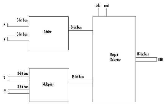
Figure 1: Mini-ALU block diagram.
2.1 8-bit Adder
Figure 2 shows the block diagram of the 8-bit adder. The adder is made of full adder blocks connected as shown in Figure 2.
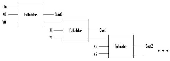
Figure 2: Block diagram of 8-bit adder.
2.1.1 Full Adder
Figure 3 shows a circuit representation of the full adder. The circuit utilizes only 2-input gates and is therefore cheaper and more are efficient.
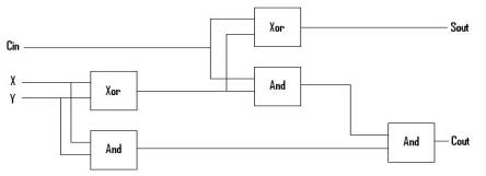
Figure 3: Circuit diagram of full adder.
2.2 8-bit Multiplier
The 8-bit multiplier consists of two blocks, the up block and the down block. They are both responsible for performing the partial additions that form the multiplication result. Figure 4 shows a block diagram of the multiplier. Only a portion of the whole block diagram is shown for clarity. The up block and the down block are presented in the next subsections.
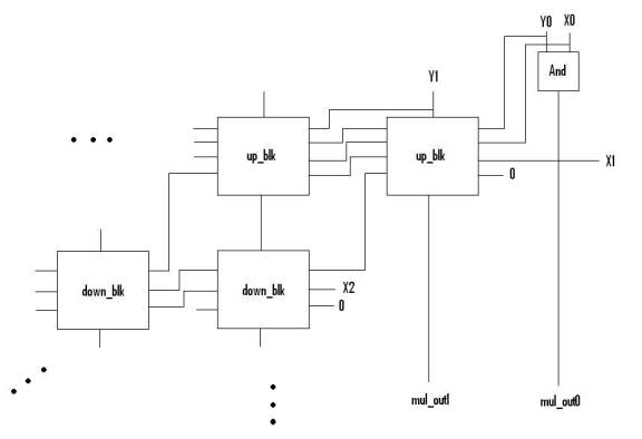
Figure 4: Block diagram of 8-bit multiplier.
2.2.1 Up Block
The up block is shown in Figure 5. It consists of one full adder block and two AND gates.
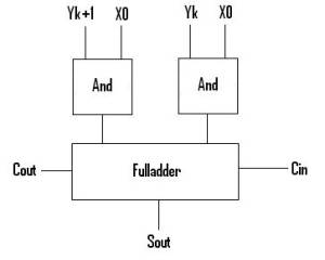
Figure 5: Block diagram of an up block.
2.2.2 Down Block
The down block is shown in Figure 6. It consists of one full adder block and one AND gate.
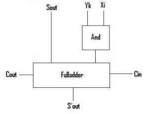
Figure 6: Block diagram of a down block.
2.3 Output Selector
The output selector block is responsible for projecting the result of the adder or the multiplier at the output of the Mini-ALU based on two control signals. Table 1 shows a truth table representation of the control signals and the functionality of the output selector block.
Table 1: Truth table representation of the output selector functionality.
|
Add |
Mul |
Mini-ALU Output |
|
0 |
0 |
0 |
|
0 |
1 |
Output of Multiplier |
|
1 |
0 |
Output of Adder |
|
1 |
1 |
0 |
The above functionality can be easily implemented by using 16 4 to 1 multiplexers and tying the necessary inputs to VSS.
3 Mini-ALU Testing
Digital circuits are normally tested using Automated Test Pattern Generation programs. These programs generate the minimum amount of necessary input vectors in order to determine possible faults in the chip. Thus, they offer the advantage of a faster and more efficient testing process. ATPG programs are based on certain fault models such as single stuck-at fault, stuck open fault, bridging fault, delay fault, etc. ATPG programs are very complicated and not well developed for some types of faults [1]. The only fault model that has well-developed and reliable ATPG programs is the single stuck-at fault model.
The other option for testing digital circuits is the exhaustive test algorithms, which applies all the possible combinations of input signals. Exhaustive testing is guaranteed to find 100% of all faults, but sometimes it might take impractically long to perform such tests. Based on practical data obtained from [1], it was determined that exhaustive testing takes 26 ms to fully test the Mini-ALU, which is a very short time. For this reason, the exhaustive test procedure was implemented.
The test procedure was comparing the output of the gate level Mini-ALU netlist against the output of another Mini-ALU netlist implemented using arithmetic operators. If the outputs of both netlists would not match, then a flag signal “CMP” would go to “1” indicating a fault for the applied combination of inputs. The results of the test procedure are shown in Figure 7.
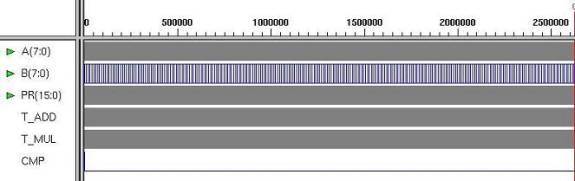
Figure 7: Simulation results of the exhaustive test procedure for the Mini-ALU.
The “CMP” signal in Figure 7 shows that the outputs of the two netlists match for all combinations of inputs indicating that the functional performance of the Mini-ALU is as expected.
4 Mini-ALU Layout
This section presents the layout floor plan and the layouts of the Mini-ALU core layout and the final layout within a pad frame. These are presented in Figure 8 to Figure 10 respectively.
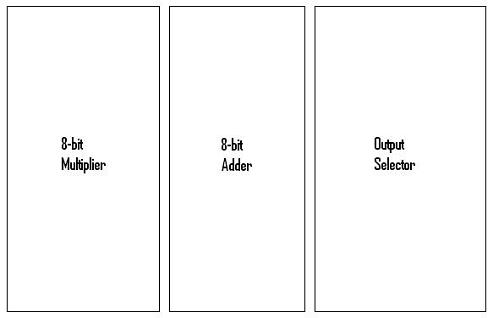
Figure 8: Layout floorplan.
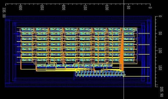
Figure 9: Core layout of Mini-ALU.
The top block of the core layout is the multiplier block. The other two blocks below the multiplier are the adder and output selector respectively. The area of the core is 355X205.9 microns.
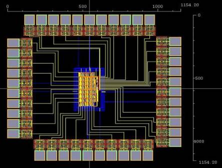
Figure 10: Layout of the Mini-ALU core within a padframe.
The pads used to create the pad frame shown in Figure 10 are the PSHORT, PSHORTVDD and PSHORTVSS found in the CMCshare library in cmosp18 technology. The pad frame design was done in four segments and each segment has its own VDD and VSS pad. The X and Y input vectors are connected to the top and left segments respectively. The “add” and “mul” control signals and the outputs are connected to the right and bottom segments.
Figure 10 shows that the Mini-ALU layout is pad frame limited due to its large number of inputs and outputs. However, if the Mini-ALU were to be manufactured, it would most likely be a sub-block in a greater chip that would require arithmetic computations.
Appendix 1 shows another implementation of the Mini-ALU using the auto-routing tools present in Cadence. The high level netlist was loaded into the Synopsys design analyzer and optimized for area. Then, another gate level netlist was generated and loaded into Encounter, which completed the layout. Figure A1 in Appendix 1 depicts the auto-routed Mini-ALU layout. The area of the auto-routed layout is 203.9X188.4 microns.
5 Layout vs.
Schematic
The Layout vs. Schematic (LVS) process was done systematically starting with the basic blocks of the Mini-ALU such as the full adder, up block and down block. Each major component was verified using DRC and LVS before it was integrated in the core Mini-ALU layout. The final LVS report of the Mini-ALU within a pad frame can be found in Appendix 2.
Appendix 1
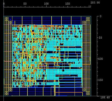
Figure A1: Core layout of auto routed Mini-ALU.
Appendix 2
@(#)$CDS: LVS version 5.0.0 08/17/2004 10:15 (cds12107) $
Command line: /nfs/vrg/cmc/cmc/tools/cadence.2003a/IC5033USR3/tools.sun4v/dfII/bin/32bit/LVS -dir /bilas/r/r2/shehuedv/cmosp18/LVS -l -s -t /bilas/r/r2/shehuedv/cmosp18/LVS/layout /bilas/r/r2/shehuedv/cmosp18/LVS/schematic
Like matching is enabled.
Net swapping is enabled.
Using terminal names as correspondence points.
Net-list summary for /bilas/r/r2/shehuedv/cmosp18/LVS/layout/netlist
count
471 nets
2 terminals
34 PSHORT
192 NAN2D0
16 MUX4D1
65 AND2D0
128 EXOR2D1
4 PVSSSHORT
4 PVDDSHORT
Net-list summary for /bilas/r/r2/shehuedv/cmosp18/LVS/schematic/netlist
count
471 nets
2 terminals
34 PSHORT
192 NAN2D0
16 MUX4D1
65 AND2D0
128 EXOR2D1
4 PVSSSHORT
4 PVDDSHORT
Terminal correspondence points
N60 N44 VDD
N123 N85 VSS
The net-lists match.
layout schematic
instances
un-matched 0 0
rewired 0 0
size errors 0 0
pruned 0 0
active 443 443
total 443 443
nets
un-matched 0 0
merged 0 0
pruned 0 0
active 471 471
total 471 471
terminals
un-matched 0 0
matched but
different type 0 0
total 2 2
Probe files from /bilas/r/r2/shehuedv/cmosp18/LVS/schematic
devbad.out:
netbad.out:
mergenet.out:
termbad.out:
prunenet.out:
prunedev.out:
audit.out:
Probe files from /bilas/r/r2/shehuedv/cmosp18/LVS/layout
devbad.out:
netbad.out:
mergenet.out:
termbad.out:
prunenet.out:
prunedev.out:
audit.out: