Scaling down to Planck's length?
In the early 1990's the commonly held opinion among scientists and engineers was that CMOS scaling (and Moore's law) would stop at 100 nm because of limitations due to fundamental device physics.
In 2007, production CMOS technology has reached the 45-nm node with physical transistor gate lengths smaller than 32 nm. MOSFETs with 1.5nm gate lengths are considered physically possible. Most foundries are concerned about economics, more than device physics, being the show-stopper for Moore's law.
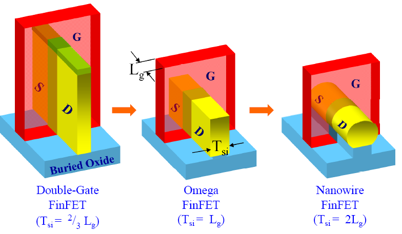
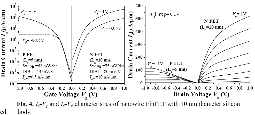
At the 2004 IEEE VLSI Technology Symposium, researchers from TSMC, Taiwan, demonstrated p-channel and n-channel nanowire MOSFETs (see figure below) with 5nm gate length and 1nm thick gate oxide. Their DC I-V characteristics, apart from the 1V bias supply, look pretty similar to the first 20V, 20um long MOSFETs that Andrew Grove, the founder of Intel, worked with in the early 1960's (see Andrew Grove, Keynote Address at IEDM 2002). Perhaps intriguingly, no quantum effects are apparent in the room temperature characteristics of these nano-scale MOSFETs which contain several thousand silicon atoms and whose channel is a quantum wire with a radius of 5nm.
Not to be outdone, during the last 10 years, theoretical physicists have not only been thinking “outside the box”, they have been searching outside this Universe, busily trying to link Shannon's theory of information, and information entropy, with string theory, loop quantum gravity and Planck's length, as the ultimate foundations of the “multiverse.” According to some of them, the maximum amount of information that can be stored in a sphere 1 centimeter in diameter is actually contained on its surface (no need for 3-D integration!) and is equal to 1066 bits, roughly the same as the inverse of one square Planck length, the quanta of the discrete spacetime. Planck's length is 1.6*10-33 cm. If only Shannon knew what he was unleashing! (Scientific American, volume 15, Number 3, 2005, Special Issue on The Frontiers of Physics).
While not quite attempting to build the “device to traverse the multiverse” - after all there still are 26 orders of magnitude between 1 nm and Planck's length – this research will investigate the physics of “down-to-earth” 1nm to 5nm semiconductor devices. The latter cannot be described by today's classical set of semiconductor equations, yet were developed based on traditional thinking by engineers who, like the bumblebee, did what they were not supposed to be able to.
The lesson here is that all we need is the vision, the belief that we can do it, and the International Technology Roadmap for Semiconductors (ITRS an industrial body of leading semiconductor foundries) to meet every two years to chart Moore's law for the next 26 decades down to Planck's length. Who said there was no future in electrical engineering?
Pictures from: Fu-Liang et al. “5nm-Gate nanowire FinFET,” 2004 IEEE Symposium on VLSI Technology Digest, pp.196-197, 2004
Sorin Voinigescu,
January 2006
Updated July 2007