ECE243
Andreas Moshovos
Revised Oct. 2015
Revised Jan 2024
Introduction
to Devices – General Concepts – Memory Mapped I/O
Having discussed
instructions and how these can be used to manipulate data in memory and
registers we now move on to how a processor can interact with the physical
world via Devices. If you recall in our first lecture
we explained that what makes computers really useful is that they can, with the
help of specialized devices, interact with the physical world.
Following
the same approach as the one we used for explaining machine instructions,
memory and registers we will first discuss the programming model for a
specific device. That is, initially we will ignore how the device works, and
focus on how it behaves. Initially, for us the device will be a black
box which we can program following the programming model. Later on we will discuss the implementation of the device.
This how it works and as we explained
earlier, there may be many different implementations that adhere to the
programming model.
The
difficulty with devices is that there isn’t a universal programming model that
can be applied to all devices. While there may be some minor similarities
for the most part most devices are specialized units
and their programming model differs significantly from those of other devices.
For this reason, we will start with a specific example and then point to some
underlying principles that are used by most devices. The example we will use is
a parallel interface (PIT) or
the General Purpose Input/Output ports
(we’ll stick to the term PIT in this note).
Before
we proceed to discuss the PITs as they is used in the
DE2 board we will first discuss how the processor can talk to a PIT and read or
write data from/to it. For this purpose let us first
define the term name space. A name space is a set of names that the
processor can access (read from or write to) using instructions. Thus far we
have seen two name spaces: memory and registers. In NIOS II the memory name
space (the address space) comprises 4G different addresses while the register
name space includes r0-r31 plus the control registers. \
In
many processors and computers that exist today, including the NIOS II, the
memory name space is also used to communicate with devices. That is, some
memory addresses are reserved at design time for accessing I/O (input/output)
devices. This way, we can access devices using the same instructions that
access memory (e.g., ldwio or stwio).
The semantics of the resulting “memory” reads and writes are device specific as
we are no longer accessing memory. In
this note we will see that by writing to one of the PITs we can turn on and off
LEDs (lights), whereas reading from another PIT we can detect whether a user pressing some of the buttons on the board.
As
a side note, please do be aware that some processors have a third, separate
name space, for accessing devices. A notable example is the x86 family (Core
Duo belongs in this family) where there are three name spaces: (1) registers,
(2) memory, and (3) devices. In such machines, there are additional
instructions for accessing devices (called IN and OUT in x86). However, most
processors and computers today use MEMORY MAPPED I/O. In memory mapped
I/O devices appear as memory addresses and can be accessed using the same
instructions that access memory. We will later explain how memory mapped I/O
works at the physical level. For the time being suffices to consider that some
addresses are NOT mapped to memory elements but to I/O devices.
The
Parallel Interface
On
the DE2 board there are several PIT devices. Let’s us
first the general form of a PIT device and then we will consider the two PIT
devices used to access the LEDs and the button switches.
In
general, each PIT can provide up to 32 external connections which can be
INPUTS, OUTPUTS, or BI-DIRECTIONAL. A bi-directional connection is one which we
can program to act as input or output, this in contrast to connections that are
hard-wired as inputs or outputs whose directionality is etched on stone at
design time. Each connection is used as
digital input or output. At the physical level what we can read or write is the
voltage level. At the time of this writing, a wire is considered by NIOS II to
be a logical 0 if it is at 0v, and it is perceived as logical 1 if it is at
3.3v.
General Form of a PIT: In the most general form a PIT
comprises 4 words in memory. We will refer to these words as “registers” and
you will often see literature for devices referring to registers comprising the
device. I am placing the word “register” in quotes as it is important to note
that sometimes these will be actual registers (as in a collection of flip-flops
you can read and write) and in other cases they might not be. Let us try to
clarify this a bit more: we would expect when we write a value v to a register,
to also be able to read back the value from it. That is, we would expect
registers to behave as storage: we write a value v, then we can read back the
value v, identical to memory values. This is not always true for device
“registers”. We shall see an example shortly.
OK,
back to the general form of a PIT device. The PIT device programmatically
appears as 4 32b registers mapped onto memory. Say the base address for the PIT
was 0x1000 (this is an example, there is not PIT there
in our system). Then there would be the following four registers:
|
+0 |
DR |
|
+4 |
DIR |
|
+8 |
MASK |
|
+12 |
EDGE |
At offset
+0 from the base address is the DR, the DATA Register, which provides a direct
connection to the wires. By reading this register NIOS II gets a snapshot of
the voltages that are present, at that moment on the wires. This is for
connections (wires) that are configured as inputs. By writing to DR, NIOS II
can force the corresponding wires to either 0v (logical 0) or Vdd (logical 1).
DIR is
the DIRECTION register. For those PITs whose connections are bidirectional,
NIOS II can write to this register and configure the connections to be either
inputs (set the bit to 0) or outputs (set the bit to 1). We discuss
these PITs later in this note.
The
MASK register is used in conjunction with the EDGE register to trigger
interrupts (we have not yet discussed what interrupts are) when an input
connection transitions from 0 to 1. We will return to the MASK registers and
interrupts later in the notes. So, we leave this for
the time being.
Finally,
the EDGE register is used to capture transitions of 0 to 1 in an input. They
are designed like to capture events of interest and we
will discuss they use in the context of the button switches. Before we do so,
let’s look at a simple example.
On our
system there is PIT whose connections are outputs and are connected to the
LEDs. The LED PIT is at base address 0xFF200000. On our boards there are only
10 LEDS, so only bits 0 through 9 are connected. By writing the DR of this PIT,
NIOS II can turn on and off the LEDs. For example, the code below, turns on the
right most 5 LEDS:
LED5off5on:
movia r8, 0xFF200000
movi r2, 0x1F # bits 4-0 are 1, all others are 0
stwio r2, 0(r8) # write the DR of the LED PIT
ldwio r4, 0(r8) # no needed, illustrates that we can also read the DR
The
last instruction (ldwio) reads the DR of the LED PIT.
While the PIT is configured as an output, it is legal to read DR and what we
get back is effectively the value that corresponds to the voltages on the
connections. In this case, these match exactly the ones we set with the earlier
stwio. So, in this case, the DR behaves like a
register that we can simply read and write.
There
is no DIR register that we need to access and configure since the LED PIT is to
be used as an OUTPUT PIT.
Stwio and ldwio
vs stw and ldw: Notice that we used stwio and not a plan stw. We will
explain the reason why in more detail when we talk about caches. For the time
being suffices to say that stwio instructs the
hardware to send a write request all the way to the actual memory or device.
Regular stw and ldw may not
necessarily reach all the way to memory as the processor has a “clever” piece
of hardware that may defer sending the request to memory or device. By using stwio or ldwio we are asking the
hardware to send the request all the way to memory or the device.
The
Push-Button PIT:
There
is another INPUT PIT starting at address 0xFF200050 which can be used to access
the four push buttons on the board. By accessing the DR register of this PIT
NIOS II can get a snapshot of which buttons are pressed. Since there are only
four buttons only bits 0 through 3 are meaningful. When a button is pressed,
the corresponding DR bit will read as 1, otherwise it will read as 0. The
following code reads the DR of the BUTTON PIT and displays the status of the
four buttons using the LED PIT
BUTTONS:
movia r8, 0xFF200000 #LED PIT/OUTPUT
movia r9, 0xFF200050 #BUTTON PIT/INPUT
FEVER:
ldwio r2, 0(r9) #read BUTTON PIT DR
stwio r2, 0(r8) # write the DR of the LED PIT
br FEVER
Stop
lying… How many times did you press it?
Time to
dive deeper into the realities of mechanical buttons and switches. The physical
circuit with the buttons is shown below:
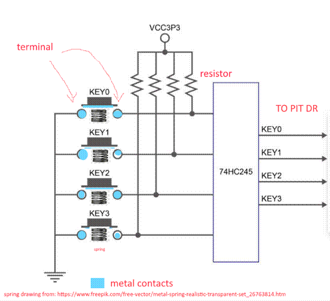
Each
button has two terminals. One of the terminals is permanently connected to ground (0v). The other terminal is connected via a resistor
to VDD (VCC in the diagram). What NIOS II accesses when it reads the DR, is the
state of the KEYx wires in the diagram (more on this
shortly). The 74HC245 chip shown contains 4 inverters (with special electrical
characteristics that are not as important to our discussion for the moment).
Let us
return to the button switches now. When a switch is not pressed, its two
terminals are not electrically connected, so the right terminal’s voltage is
“pulled up” to VDD via the resistor. The corresponding KEYx
output will then read as 0 since the 74HC245 passes it
through an inverter. However, when NIOS II reads the BUTTON PIT DR register,
there is one more inverter that is not shown on the diagram and as a result
NIOS II reads the inverted state of the KEYx wires.
That is, when the button is not pressed it will read as 0 to NIOS II.
When we
press a button, its two terminals are then electrically connected by the metal
plate on the underside of the button. In this case, the inputs to the 74HC245
go to 0v, and the KEYx output goes to 1. Since this
is inverted once more, NIOS II will read it as a 0.
Once we
depress the button, a spring (or an equivalent contraption, pushes the button
and the metal plate up, and the electrical connection between the two terminals
seizes. The output pulls up at Vdd again, and NIOS II
will now again read a 0 for the button (not pressed). Side note, the actual
mechanism used by the button may be different (simpler actually
as having one terminal being a simple metal plate that bends and touches
the other terminal when pressed by the button cover, and that springs back into
place on its own) but the concept holds.
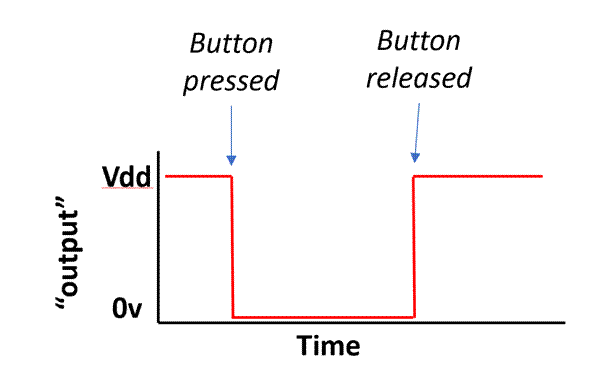
The
idealized Button behavior:
As per
the preceding description, one would naturally expect the output seen on the
right terminals to be as follows in time. In the diagram below we show the
voltage on the right terminal of one of the buttons. At rest, when the button
is not pressed, it is at Vdd, the moment we press the
button, it goes to 0v, and then the moment we release the button, it jumps up
at Vdd:
However,
this is not what happens in reality when we press the
button. The pieces of metal that are supposed to touch to create the electrical
connection between the two terminals bounce as they touch. Mind you, this
happens over a very short period of time (think
microsecs to milliseconds). So, it is not something we can perceive as humans.
However, recall that NIOS II operates at the MHz range and other processors at
the GHz range, so there could be thousands to millions of instructions that
execute during this bouncing event. If we write a program that simply reads the
DR register with the intention being for example to count how many times the
key is pressed, it will not work well for us. Each time the button is pressed
and depressed, the program will “see” the DR bits changing from 0 to 1 multiple
times.
What happens
in reality when keys are pressed is shown in the below
diagram in the “before Debouncing” diagram:
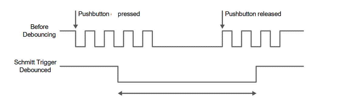
The
74HC254 inverters “filters” the signal and we get the “Schmitt Trigger
Debounced” signal on the KEYx wires. This is what an
ideal switch would behave like. If interested you can
read more about the “Schmitt Trigger” inverters that are inside the 74HC245.
These are inverters whose characteristic curve (what the output given the
input) different depending on how the input is
changing, meaning whether the input is moving from 0v to VDD or vice versa. For
a regular inverter, the direction of change matters little or none at all. For these inverters however, the direction of
change matters. In simple terms, the threshold voltage for considering the
input as 0 or 1 changes depending on the direction of change. However, knowing
how these inverters work is not needed for us to program and use the button
PIT. So, we leave it at that.
Returning
to our discussion, we note that effectively the 74HC245 chip “debounces” the
button switches. Debouncing can also be done in software (it costs having the
extra chips just for debouncing and the costs grow with the number of buttons
we have). Debouncing in software is explained later on
in these notes and in the context of the general purpose I/O PIT.
Using
the EDGE register: An example Toggling a LED
Now,
we can discuss the use of the EDGE register. The EDGE register captures the
0->1 edge on the KEYx wires. Each bit of the EDGE
register corresponds to one of the KEYx wires. It is
normally at 0. When the 0->1 edge is detected, the corresponding EDGE
register bit is set to 1. This is a sticky bit, that is, it will stay at
1 until we explicitly go and reset it. So, an EDGE register bit gives us the
following information when it reads as 1. At some point in time before we read
it, the button was pressed AND released.
How
do we reset an EDGE bit that was set to 1 by pressing a button? We do that by
writing 1 to it. Here’s an example code that illustrates the use of EDGE bits.
The code is an infinite loop that checks whether the first button was pressed
and turns the first LED on and off. Every time we press the button, the LED
will toggle.
ButtonToggleLED:
movia r8, 0xFF200000 #LED PIT/OUTPUT
movia r9, 0xFF200050 #BUTTON PIT/INPUT
stwio r0, 0(r8) # turn off all LEDs, write 0 to LED PIT DR
FEVER:
ldwio r2, 12(r9) #read BUTTON PIT EDGE
andi r2, r2, 1 # check bit 0
beq r2, r0, FEVER # not pressed yet, keep checking
# button has been pressed and released at some point
pressed:
ldwio r4, 0(r8) # read LED DR (current status)
xori r4, r4, 1 # toggle led 0
stwio r4, 0(r8) # change the LEDs (write to LED PIT DR)
movi r2, 1 # RESET bit 0 of BUTTON PIT EDGE
stwio r2, 12(r9) # write the DR of the LED PIT
br FEVER
Using
C To Program the PITs
We do
not necessarily need to write assembly to communicate with the PITs.
The
following C code for example turns on all LEDs by accessing the LED PIT DR
using a pointer:
#define LED_DR ((volatile unsigned int *)
0xFF200000)
void
main (void)
{
*LED_DR = 0x3F;
}
The
volatile keyword tells the compiler not to use a register to hold the value at any
point. Instead all reads and
writes should be done by following the point and accessing “memory” using stwio or ldwio.
Recall
the PIT, in its general form, contains 4 registers. We can use a C structure to
make our code easier to maintain and to understand:
// A PIT appears as four
consecutive words in memory
struct PIT_t {
volatile unsigned int DR;
volatile unsigned int DIR;
volatile unsigned int MASK;
volatile unsigned int EDGE;
};
// The LED pit is at this
base address
struct PIT_t *ledp = ((struct PIT_t *) 0xFF200000);
// The BUTTONS pit is at
this base address
struct PIT_t *buttonp = ((struct PIT_t *) 0xFF200050);
void
LEDtoggle(void) {
ledp->DR
= 0; // turn off all leds
while (1) {
// check if the first button was pressed and released
if (buttonp->EDGE
& 0x1) {
ledp->DR
= ledp->DR ^ 0x1; // toggle bit 0 of the leds
buttonp->EDGE
= 0x1; // reset bit 0 of the BUTTON EDGE
}
}
}
The General Purpose PITs
(GPIO)
On the DE2 board there are two
PIT devices called GPIO 1 and GPIO 2. Each provides 32 external connections
named as D0 through D31. These connections are called General Purpose I/O pins because each is a single wire which can be used as digital input or output. Under program control we
can either read the logical level at each of those wires (i.e., whether the
voltage on that wire is a logical 1 or a logical 0) or set their voltage to
logical 0 or logical 1.
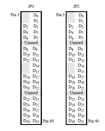
Physically the GPIO pins appear on the JP1 and JP2 connectors on the boards. Here’s a diagram of how the pins are connected (the gray boxes correspond to pins that are not used by the port – they are connected to the power supply rails):
As an example we will consider an application where the PIT is used to control the fan of a heating system. The PIT will be used to read the status of a thermostat and then it will be used to turn on or off the heating system’s fan. We will assume that the thermostat provides a single output which is 0 if the temperature is less than a preset level and 1 otherwise. We want to turn of the fan is the thermostat’s output is 0 and turn it off otherwise (you may observe that a computer is probably an overkill for this application, however, please recall this is an example). So, one of eight PIT connections will be used as input to read the thermostat status and another will be used as output to control the fan motor.
The PIT interface presents a programming interface that consists of two bytes in memory (there are more registers which we will describe later on). For port GPIO 1 the two registers are:
The DATA register (DR) at address 0xFF200060 (read or write)
The DATA DIRECTION register (DIR) at address 0xFF200060 + 4 = 0xFF200064 (read or write)
|
Address |
WORD |
|
|
0xFF200060 |
DR |
Data Register |
|
0xFF200064 |
DIR |
Direction Register |
We can view the device as having a base address of 0xFF200060, and the two registers at offsets (distances) +0 for DR and +4 for DIR. The other PIT is identical using only a different base address. Here’s the complete list:
1. PIT 1: 0xFF200060
2. PIT 2: 0xFF200070
In addition to the two registers we just described each PIT has two more registers which are used to control the port’s interrupt behavior. More on this when we start discussing interrupts.
As we noted earlier the PIT provides 32 external single “bit” (wire) connections to the outside world.
Each of these connections can be configured as an input or an output independently. This can be done by writing a value into the DDR register. The DIR register has 32 bits which we can change by storing a word into the address where DIR is mapped at. Each of these bits controls the direction of the corresponding external connection. For example, if bit 0 of DIR is set to 1, then D0 becomes an output otherwise it becomes an input. When we access an I/O device we *have* to use the IO variants of loads and stores, e.g., ldwio or stwio. These instructions bypass any temporary buffering that the CPU may be performing and send the memory requests immediately.
Here are a couple of example of configuring the PIT ports for input or output:
Configure all pins as outputs
addi r8, r0, 0xFFFFFFFF
movia r9, 0xFF200064
stwio r8, 0(r9)
Configure all pins as inputs
addi r8, r0, 0
movia r9, 0xFF200064
stwio r8, 0(r9)
Configure pins D0 through D3 as outputs, and pins D4 through D31 as inputs
addi r8, r0, 0x000000F
movia r9, 0xFF200064
stwio r8, 0(r9)
To set the value of a PIT bit to a specific level we have to
write the corresponding bit of the DR register. Thus, assuming
that DIR=0xFFFFFFFF, then writing 0x0000000F into DR forces D0-D3 to
logical 1 and D4-D31 to logical 0. If a pin is configured as an input, writing
the corresponding DR bit does not change the pin’s value. Such writes are silently ignored.
At any time we can read the DR register and read the logical values of the 32 external connections. If a connection has been configured as an output we are effectively reading the value we have written in the corresponding DR bit. If a connection has been configured as an input then we are directly reading whatever value has been placed on the connection from the outside world (for example from the thermostat).
Example: Let’s us now write the program that reads the thermostat and controls the heating fan. We will assume that the thermostat is connected to bit 0 of PIT 1 (which should be configured as an input) whereas the fan is connected to bit 2 (which should be configured as an output). The thermostat outputs 0 when it’s cold and we need to turn the fan on, otherwise it outputs 0.
So:
D0 is connected to the thermostat’s output
D3 is connected to the heat fan motor
PIT_DR_OFFSET equ, 0x0 # So, DR is at PIT1_BASE + PIT_DR_OFFSET
PIT_DIR_OFFSET equ, 0x4 # and, DIR at PIT1_BASE + PIT_DIR_OFFSET
.text
heat:
movia r9, PIT1_BASE
addi r8, r0, 4
stwio r8, PIT_DIR_OFFSET(r9) # configure all pins but D3 as inputs
stwio r0, PIT_DR_OFFSET(r9) # turn off the motor
fever:
ldwio PIT_DR_OFFSET(r9), r8 # read all pins
andi r8, r8, 0x1 # mask out all but D0
beq r8, r8, fanon # if zero, then it’s cold turn the fan on
fanoff:
stwio r0, PIT_DR_OFFSET(r9) # turn fan off or keep it off
br fever
fanon:
addi r8, 4
stwio r8, PIT_DR_OFFSET(r9) # turn fan on or keep it on
br fever
In order not to forget that C provides us with most of the functionality that assembly does, here’s how the aforementioned code can also be written directly in C:
#define DR ((volatile unsigned int *) 0xFF200060)
#define DIR ((volatile unsigned int *) 0xFF200064)
void
heat (void)
{
unsigned int t;
*DIR = 0x4;
*DR = 0x0;
while (1)
{
t = *DIR;
if (t & 0x1)
*DR = 0x0;
else *DR = 0x4;
}
}
So, while programming try to avoid using assembly as much as possible. In most cases this will be possible. However, there are cases where using assembly will be important and necessary (for example, you have little control of how the compiler translates a piece of C code, hence it may use inefficient instruction sequences, moreover, since the compiler does not have an understanding of device semantics – programming model – it may use instruction sequences that have unexpected behavior such as accessing the same device register multiple times).
A cleaner/easier to read way of implementing the code in C uses a structure declaration for the device:
struct PIT_t {
volatile unsigned int DR;
volatile unsigned int DIR;
};
struct PIT_t *pitp = ((struct PIT_t *) 0xFF200060)
void
heat (void)
{
unsigned int t;
pitp->DIR = 0x4;
pitp->DR = 0x0;
while (1)
{
t = pitp->DR;
if (t & 0x1)
pitp->DR = 0x0;
else pitp->DR = 0x4;
}
}
In this code we exploit the fact that the structure elements are laid out in memory one after the one. So, the DR element appears first, occupying four bytes. Immediately, after it is DIR. This style is easier to maintain and exposes the true structure of the device. We can now use the structure to refer to the other PIT devices easily. Otherwise, we would have to write the addresses of each register explicitly every time. With the structures we only need to write the base address of each device. This style is easier to maintain also. In the documentation for the NIOS II system we use, you will see that the PIT has a couple more registers. We can expand the structure definition once to include these registers without having to change the code much.
Another Example –
Debouncing
As an additional example let us consider what happens when the thermostat uses a mechanical arrangement where metal contacts touch to report a logical 1. Whenever metal contacts are used there is a short period of time where they bounce repeatedly whenever the switch changes state. So for a short period of time what we will observe at thermostat’s output will be a series of alternating 0’s and 1’s. The NIOS II is much faster in processing instructions hence the above code will turn on and off the fan several times while the thermostat changes state. We can revise our program to reduce this or even avoid it completely. This is typically called debouncing. Here’s one way of achieving this: Rather than reading the DR once (taking a single sample of the input’s state) we read it several times counting how many times it was 1. If we took N samples and the number of those samples that was one is greater than N/2 then we can assume that the value read is 1 otherwise we can assume it is a zero. Here’s the code:
PIT1_BASE equ, 0xFF200064
PIT_DR_OFFSET equ, 0x0
PIT_DIR_OFFSET equ, 0x4
.text
heat:
movia r9, PIT1_BASE
addi r8, r0, 4
stwio r8, PIT_DIR_OFFSET(r9) # configure all pins but D3 as inputs, D3 controls the fan motor
stwio r0, PIT_DR_OFFSET(r9) # turn off the motor
fever:
addi r10, r0, 1000 # we’ll be taking a 1000 samples in r11
add r11, r0, r0 # r11 = 0
sampling:
ldwio r8, PIT_DR_OFFSET(r9) # read all pins
andi r8, r8, 0x1 # mask out all but D0, DO is the thermostat
add r11, r11, r8 # r11 = r11 + bit 0 of DR, or equivalenty if (D0 == 1) r11 = r11 +1
subi r10, r10, 1 # r10 = r10 – 1, one fewer sample needed
bne r10, r0, sampling # more samples needed
addi r10, r10, 500 # 500 is the threshold
bgt r11, r10, fanon # if more than a 500 ones turn the fan on
fanoff:
stwio r0, PIT_DR_OFFSET(r9) # turn fan off or keep it off
br fever
fanon:
addi r8, 4
stwio r8, PIT_DR_OFFSET(r9) # turn fan on or keep it on\
br fever
Please note that I have not tested this code on the DE2 so, using 1000 may not
be the best possible choice or even a good one.
The PIT Implementation
The example in this section shows a PIT with 8
external connections. Its DR register appears at location 0xFF1110 and its DIR register at location
0xFF1114. From this description you should be able to make the necessary
changes to create a 32-bit PIT at the addresses used on our system.
Having seen how to program the PIT we can now discuss one implementation. This is not necessarily how it is implemented on the DE2. At the physical level the PIT presents the following signals:
Data: a set of 8 wires that are used for supplying the value to written to registers DIR or DR, or to read the value from the DR. These signals can be used as input or as output as explained subsequently.
A DIR write
signal: When this is 1 the value in the Data is written into the DDR
What appears to software as a single register DR is implemented using separate elements for input and output. The DRO latch implements the output portion, while a tri-state buffer is used for the input portion. Here’s the diagram of one PIT bit:
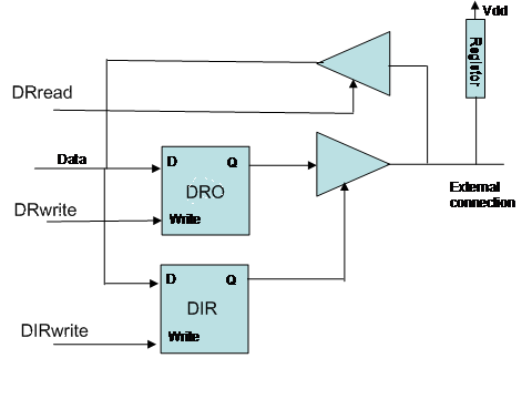
The DRO and DIR boxes are latches. We can change their value using the Data and Write signals. The DIR latch output drives a tri-state driver whose output is connected to the external connection. If DIR is 1 then the tri-state buffer behaves like a buffer and passes the value of the DRO latch to the external connection. If DIR is 0 then the tri-state buffer is placed in the off state which can be thought as an open switch (no connection). In this case, an external source will determine what the value is on the external connection wire. The resistor is there to help when DRO wants to drive a 1 (high voltage) since the technology used is not very “strong” when driving a one. The registor also sets the external connection to 1 when no one is driving it.
If DR Read becomes 1 then the upper tri-state buffer is activated and passes the value on the external connection to the data wire. What we have described is just one of the 8 slices used by the PIT. The 8 slices are connected together so that they share the Write and Read lines and so that their data lines collectively form the 8-bit data interface of the PIT.
To connect the PIT to the NIOS II processor we need to first explain what is the physical memory interface. This discussion follows. We do not discuss the exact implementation of NIOS II. Instead we present an interface that is simple enough to allow us to focus on the fundamentals.
Memory
------------------------------------------------------------------------------------
And in order to not forget that we eventually we will be talking about actual implementations let’s see how a typical memory interface will look at the physical level. This exercise will allow us to see how we can use the binary system to encode quantities other than numbers.
So, let’s start first with the vocabulary we need to be able to talk. This includes the operations and their arguments. Our goal is here to determine how many signals (i.e., bits) we will need to be able to specific these operations. We have the following operations:
Load.DataType Address
Store.DataType Data, Address
Where DataType can be any of the following three: byte, word or long-word. Address is 24 bits for 64k. And Data can be 8, 16 or 32 bits.
These requirements can be stated as follows:
Two operations: load or store
Three data types: byte, half-word or word
One address of 32 bits
One data value of at *most* 32 bits for specifying the value to write for stores
One data value of at *most* 32 bits for memory to returns the value for loads
We also need to be able to say that we do not want to read or write from/to memory, i.e., do nothing
For 1 it’s enough to use a single signal which we will call R/W’. When R/W’ = 1 then we want to perform a load, while when R/W’ = 0.
For 2, it’s enough to use two signals. Let’s call them collectively DW and use the following encoding (others possible):
DW | Data Type
----------------
00 | byte
01 | half-word
10 | not used
11 | long-word
For 3 and 4 we need 32 signals for each (or we could multiplex the same wires).
Finally for 5 we need a master-enable signal ME. When ME = 0 memory ignores all other signals. When ME = 1 then memory looks at the other signals and responds accordingly.
Besides being able to say to memory “do noting” ME plays another important role. In the physical world it takes time for us to setup coherent values on all signals. For example, assume we want to perform in sequence a STORE.BYTE 0x10, 0X000000 and a STORE.BYTE 0x01, 0xffffff. It is practically impossible to change all signals instantaneously. So, in going from address 0x000000 to 0xffffff all possible binary numbers may temporarily appear (because different signals may change at different rates). Without the ME, the memory could get confused and misinterpret the second store. With ME, we can se ME to zero in between the two stores, wait sufficient time for the second store values to appear on the data and address signals and then set ME=1. This way memory remains oblivious to temporarily inconsistent values.
Connecting the PIT to the Memory Interface
----------------------------------------------------------------------------------------------------
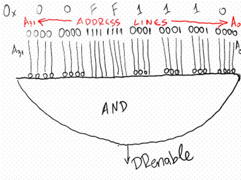
To connect the PIT to the memory interface described previously, we first connect the PIT Data lines to the lower byte (8 bits) of the memory data lines. This will allow us to access the three PIT elements (DIR, DRO and DRI) by using load and store memory accesses. Then we need to activate the corresponding PIT elements depending on the address accessed. We need to detect the following combinations on the address lines: 0xFF1110, and 0xFF1114 (this assumes that the PIT is at these addresses – it’s from an older version of the hardware – please substitute the new addresses for these 0xFF200060 and 0xFF200064). In the simplest to describe implementation we use a 32 input AND gate for each of those. Let’s see how we decode the address 0x00FF1110. Using a 32-bit input here’s how we can detect this combination on the address lines: write the number in binary. For every digit that is 1 connect the corresponding wire directly to the AND gate. For every digit that is 0, connect the corresponding wire first to inverter and then connect the output of the inverted to the AND gate.
Here’s the ADDRESS DECODING part for DR, it generate the signal DRenable that tells us that the processor is either reading or writing DR:
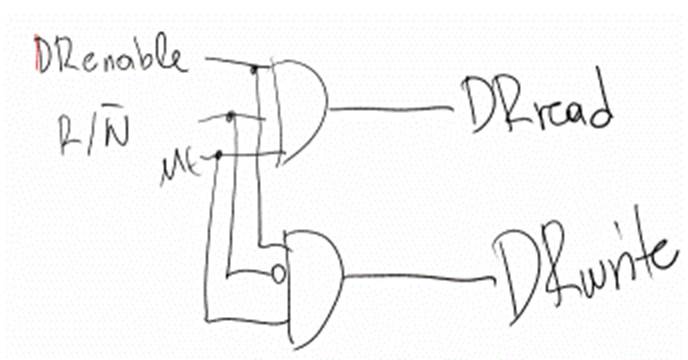
DRenable can now be combined with R/W’ and ME to generate the DRread and DRwrite signals:
Here’s the address decoding and signal generation circuit for DIRwrite:
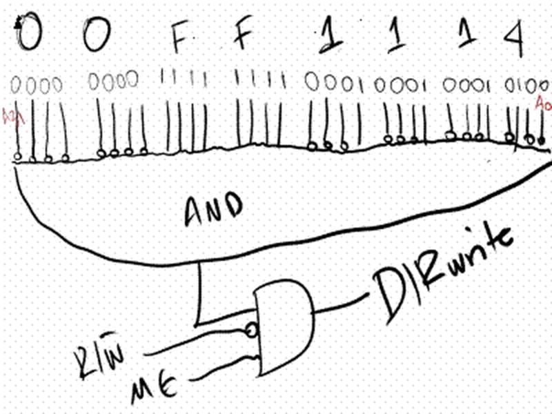
In total we used two three 32-input AND gates and three 3-input AND gates. Each of the two 32-input AND gates is connected to all 32 address signals. By using inverters appropriately we can detect that the address being accessed is one of those mapped to DR, and DIR. We start by looking at the binary representation of these addresses and put an inverter for those address bits that are zero in the pattern we are interested in. After detecting the address, we then used a 3-input AND gate to detect accordingly whether an access is being made (ME == 1 – ME is Master Enable), and whether it is a read or a write.
This implementation is easy to understand, however, it’s not necessarily the most efficient. This topic is beyond the scope of this lecture, however, you are encouraged to think of ways of reducing the number of components needed to do address decoding.
Here’s the complete design:
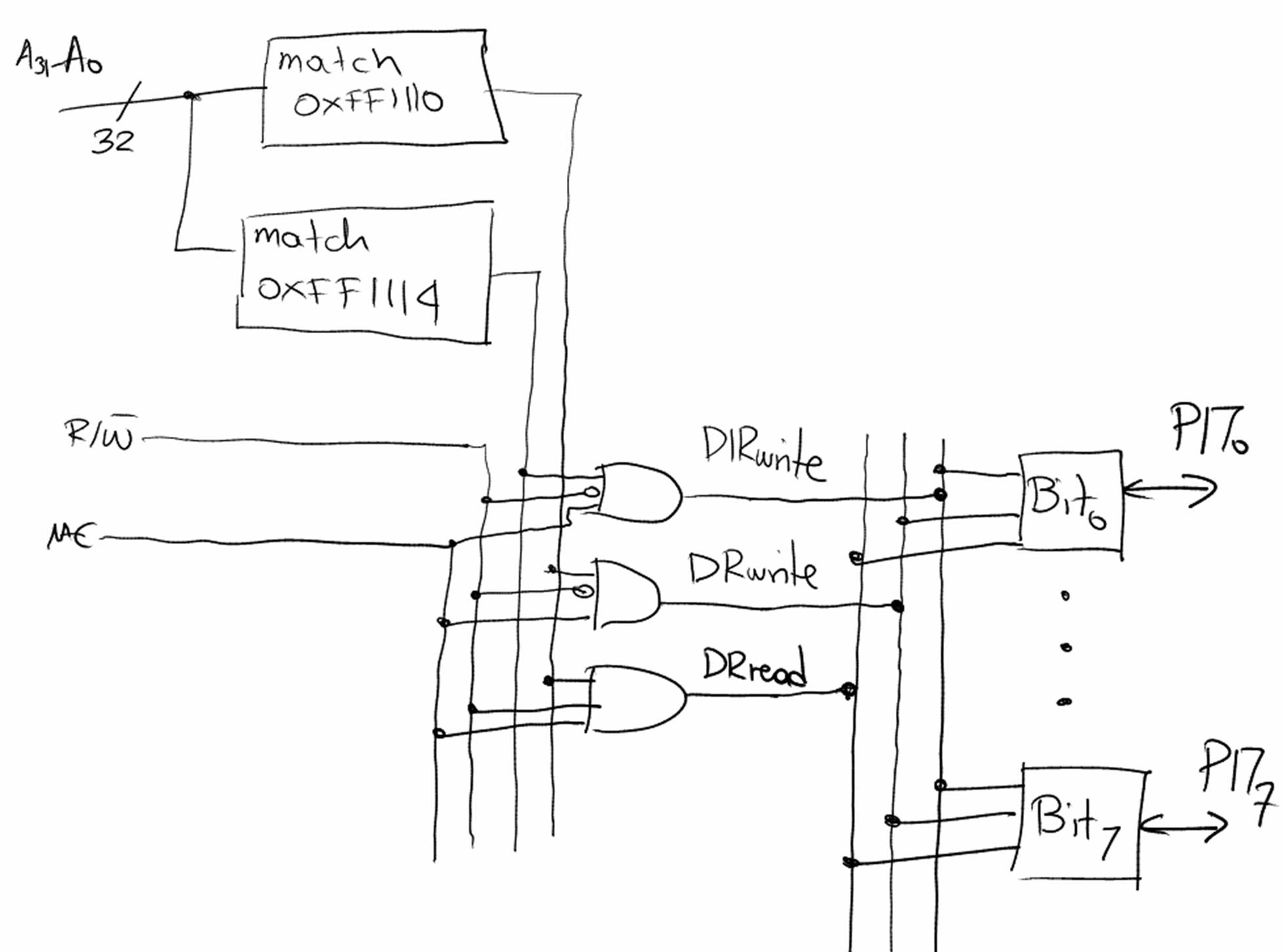
Each
bit cell (there are eight of them) is as shown earlier). The boxes labeled
“match some hex value” are the 32-bit input AND gates we described earlier.