Computer Organization
Andreas Moshovos
FALL 2013
Pipelining
Concept
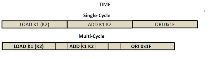
Thus far we’ve seen two different ways of implementing processors. In the first, and slower performing, each instruction took a single cycle to execute. In the second, multi-cycle implementation, each instruction took multiple, shorter cycles to execute. In either case, instructions execute in isolation in time as the time diagram below shows:
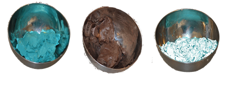
However, both approaches fail to exploit the fact that executing an instruction is not a monolithic operation. Instead, instruction execution comprises several smaller actions that ought to be performed in sequence. Let’s use a cake making analogy. Let’s say after the valuable education you receive you decide to become a purveyor of fine birthday cakes. To start, you decide you will focus on single product: shark cakes. Here’s one:

How do you make such a cake you ask? I’m glad you did. I recently made one. First you make the dough for the base and then bake it:

BTW, a nice recipe can be found here http://www.marthastewart.com/337010/chocolate-cupcakes.
You may want to cut down on the sugar, it will still taste delicious.
Once you have the
base, then comes the fun part, frosting. For that you need three frostings
colored blue, white, and black:
Recipe here: http://www.marthastewart.com/318727/swiss-meringue-buttercream-for-cupcakes.
Then in three steps,
you apply first the blue, then the white and then the black “frosting”:

So, in total, making
a cake requires five actions:
1.
Make the
dough
2.
Bake the
dough
3.
Apply
blue frosting
4.
Apply
white frosting
5.
Apply
black frosting
If you are making
one cake you would perform the actions sequentially:
You find that
business has picked up, and you can no longer keep up with demand. What can you
do to? How about this? You get four of your friends on board and now the five
of you work together:
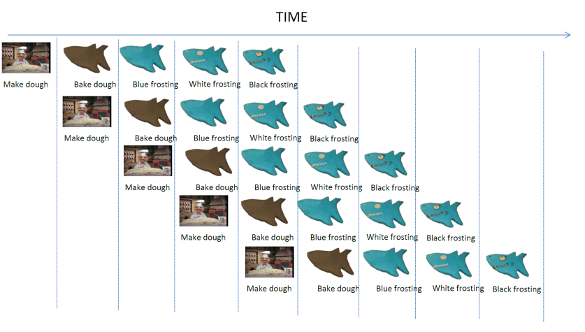
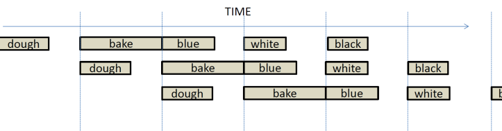
The previous time
diagram shows five cakes in the making. Each person does one thing. The first
makes the dough, the second bakes it, the third applies blue frosting and so
on. While each cake still takes five steps to make, multiple cake are been made
in parallel each being at a different stage of preparation (you may be thinking
we can do cakes in parallel – yes, that is possible but defer that thought
until we start talking about superscalar architectures). This is pipelining.
In our example, each stage takes exactly the same time and as result each
cake takes almost exactly the same time to be made as before and because we partially overlap the making of many cakes,
we do made more cakes over the same amount of time. That is the cake throughput,
defined as #cakes/time is higher. The reality is, however, that the stages
will require different amounts of time. In this case, the longer stage will
determine the rate at which the pipeline will work as shown in the following
diagram:
In this example, baking a cake takes much longer than every other step. So, our
pipeline now proceeds in stages each taking the same amount of time as baking
the cake. Except for baking, all other actions finish early in their respective
stages and then they wait. This is necessary since we assume that we only have
one oven. While this way it takes longer to make each cake the cake throughput
is still higher than it was compared to making one cake at a time.
Pipelining Instruction Execution
Pipelining can be
applied to many activities including instruction execution. Instead of
approaching instruction execution as a monolithic sequence of actions that have
to happen one at a time, we can approach instruction execution as a series of
steps, or stages that can be partially overlapped
across instructions. Applying pipelining
for instruction execution will be a bit more tricky than for baking cakes for
the following reasons:
1.
Instructions
may produce results that other instructions may use. That is, instructions have
data dependencies. No cake depends on another cake.
2.
Instructions
may change the PC and hence may change which instructions will execute next.
These are control dependencies. When we were making cakes, we knew which
cakes we will make in advance.
3.
Instructions
may produce results at different execution stages. We have to be wary to adhere
to sequential semantics so that the program still runs correctly.
4.
Instructions
need resources to execute, such as ALUs, registers, memory, etc. Same with
cakes, but for our example, we made things simple by assuming we had enough of
those.
5.
While this
is not possible in our architecture, instruction execution may have to be
stopped due to exceptions. For example, in NIOS II this may be a division by
zero, or an unaligned memory store or load.
For the time being,
let’s ignore these issues and let’s assume that somehow we will be executing
straight-line code (that is PC next = PC + 1 always). We will progressively
refine our implementation to tackle all aforementioned challenges.
To start building
our pipeline, let’s start simple by trying to pipeline just the ADD, SUB, and
NAND instructions. These are structurally similar, the only thing that changes
is what calculation they perform in the ALU.
Let’s recall how these are implemented in our multi-cycle implementation.
The following table
shows the execution steps for all instructions as we have optimized them:
|
CYCLE |
|
|
|
ADD, SUB, NAND |
|
1 |
[IR] = Mem[ [PC] ] [PC] = [PC] + 1 |
|
2 |
[R1] = RF[ [IR7..6] ] [R2] = RF[ [IR5..4] ] |
|
3 |
[ALUout] = [R1] op [R2] Update Z & N |
|
4 |
RF[ [IR7..6] ] = [ALUout] |
Recall that the
aforementioned schedule relies on speculation and data dependencies to reduce
the number cycles needed to four.
Without speculation, the schedule required five cycles:
|
CYCLE |
|
|
|
ADD, SUB, NAND |
|
1 |
[IR] = Mem[ [PC] ] [PC] = [PC] + 1 |
|
2 |
Decode |
|
3 |
[R1] = RF[ [IR7..6] ] [R2] = RF[ [IR5..4] ] |
|
4 |
[ALUout] = [R1] op [R2] Update Z & N |
|
5 |
RF[ [IR7..6] ] = [ALUout] |
We’ll start with this
5-cycle schedule to build our pipeline since it is easier to understand. It is
possible to use speculation to reduce the number of stages but that would
require corrective action for ORI. We may discuss this later.
The aforementioned
five cycle schedule for ADD, SUB and NAND can be distilled down to the
following five stages:
1.
FETCH:
Fetch Instruction and update PC (PC = PC + 1)
2.
DECODE:
Decode Instruction
3.
RF: Read
Registers or Update PC for branches
4.
EXEC:
Execute and Memory Read and Memory Write
5.
WB: Writeback
results to Register file
The following table
names these stages and details what actions take place:
|
CYCLE |
|
|
|
|
|
ADD, SUB, NAND |
|
1 |
FETCH |
[IR] = Mem[ [PC] ] [PC] = [PC] + 1 |
|
2 |
DECODE |
Decode |
|
3 |
RF |
[R1] = RF[ [IR7..6] ] [R2] = RF[ [IR5..4] ] |
|
4 |
EXEC |
[ALUout] = [R1] op [R2] Update Z & N |
|
5 |
WB |
RF[ [IR7..6] ] = [ALUout] |
In time, we have the
following diagram showing 6 instruction, I1 through I6, executing in a
pipelined fashion:
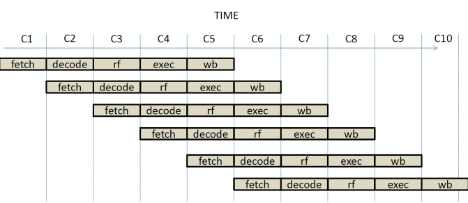
In C1, I1 is being
fetched. In C2, I1 is being decoded while in parallel, I2 is being fetched. In
C3, I1 is reading from the register file, I2 is being decoded, and I3 is being
fetched, and so on. Let’s focus on C5: In C5 we have five instructions being
executed in parallel, each at a different stage of their execution:
1.
I1 is finishing writing its result back to the
register.
2.
I2 is
performing a calculation in the ALU.
3.
I3 is reading
registers from the register file.
4.
I4 is
being decoded.
5.
I5 is
being fetched from memory and updating the PC.
Notice that at every
stage of the pipeline there are different actions. What action needs to take
place depends on the instruction executing at that stage alone. So each stage needs to operate independently,
and at the end of each cycle each stage will pass work to the next stage down
the pipeline. As a result, our pipelined implementation will look as follows:
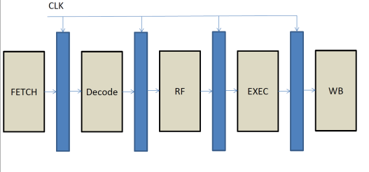
Each stage has a
combinatorial component that performs the calculations necessary and in between
the pipeline stages there are registers. These registers act as an output for
one stage, and as an input for the next stage. At the end of the clock cycle,
the results of each stage are loaded into the output register for the stage.
These are then used as inputs for the next stage during the next cycle. The FETCH stage has no input register since
it uses the PC as the only input.
Let us now see how
we can implement this in hardware. Let’s start with the multi-cycle datapath
and to make things easier to follow assume that we executing the following
instruction sequence:
I1: ADD K1 K1
I2: SUB K2 K2
I3: NAND K3 K3
I4: ADD K0 K0
I5: SUB K2 K1
FETCH stage:
We can start from
our multi-cycle implementation. Let’s start building the pipeline stage by
stage. In stage 1, we need to fetch an instruction and update the PC. In the
multicycle implementation this is done
as shown below:
At the end of the
cycle the new instruction will be loaded into the IR register can act as the
pipeline stage register between the FETCH and DECODE stages. While in the multi-cycle
implementation we could use the main ALU to do PC = PC + 1, this is not
possible in the pipelined implementation since that ALU will be used to
implement the EXEC stage. This is a structural hazard. A structural
hazard occurs when at least two different stages attempt to use the same
resource. Since the stages operate concurrently, this is not possible. One
solution to such structural hazards is replication. If a resource cannot be
shared, we can use a second copy to accommodate another stage. In our case, we
can provide a dedicated adder for incrementing the PC in the FETCH stage. Our datapath now looks as follows:
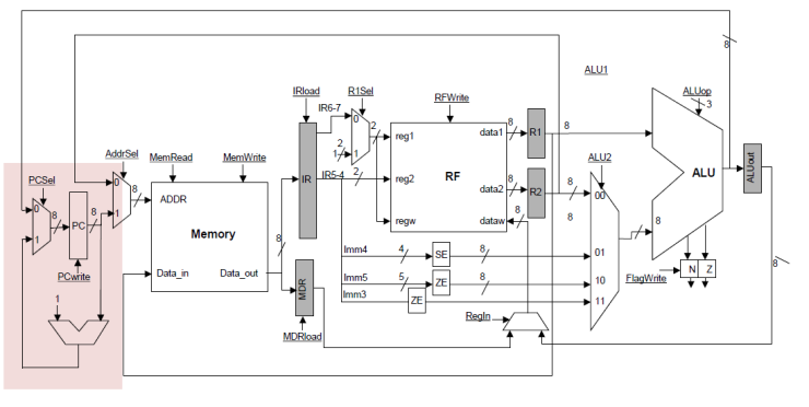
During the FETCH
stage, the PC can become PC + 1 and an instruction can be fetched into IR.
DECODE stage:
Next comes the
DECODE stage. Nothing happens in the datapath during this stage, the control is
taking a look at the instruction just fetched and prepares the next set of
actions that will happen in the RF stage. Since a cycle does elapse and another
instruction is being fetched, we need a register to pass along the previous IR
to the RF stage while allowing a new IR to be loaded with the next instruction.
Our datapath now is as follows:
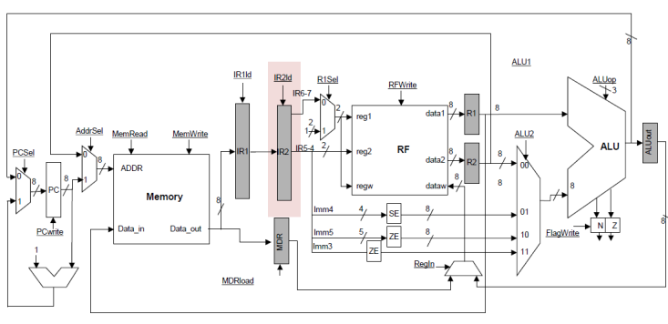
RF Stage:
In the stage 3, the
RF stage, we can now proceed to read the two registers as specified by the
instruction. For this purpose, we are using the instruction stored in the IR2
register which is the one that was
provided by the DECODE stage:
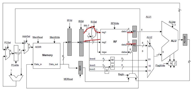
The existing R1 and
R2 registers can act as the register between the RF and the EXECUTE
stages. The EXEC stage also needs to
know what operation to perform and finally, we need to remember which register
we need to be writing to when we eventually arrive at the WB stage.
Accordingly, we can add on more IR register as shown below. Alternatively, we
can pass along all the necessary information encoded in a convenient form. For
example, we can use an alternate encoding for the operation, etc.
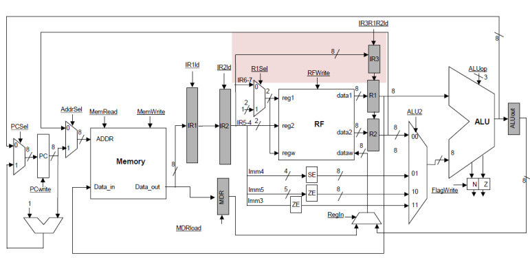
EXECUTE stage:
In the fourth,
EXECUTE stage, the calculation takes place in the ALU and we update the Z and N
flags:
As before, this is
not sufficient, we also need to pass along some information to the next stage
WB so that it can write the result back to the appropriate register. For this
purpose we can simply introduce another IR register as shown below:
WB stage:
In the fifth and
final WB stage, the result previously calculated into ALUout gets written into
the register file. The register name now
has to come from IR register that is between EXEC and WB. That would be IR4 in
our not so great naming scheme:
We have now seen how
a single ADD, SUB or NAND instruction will flow through a simple 5-stage
pipeline. However, as designed our pipeline has problems. We discuss those
next.
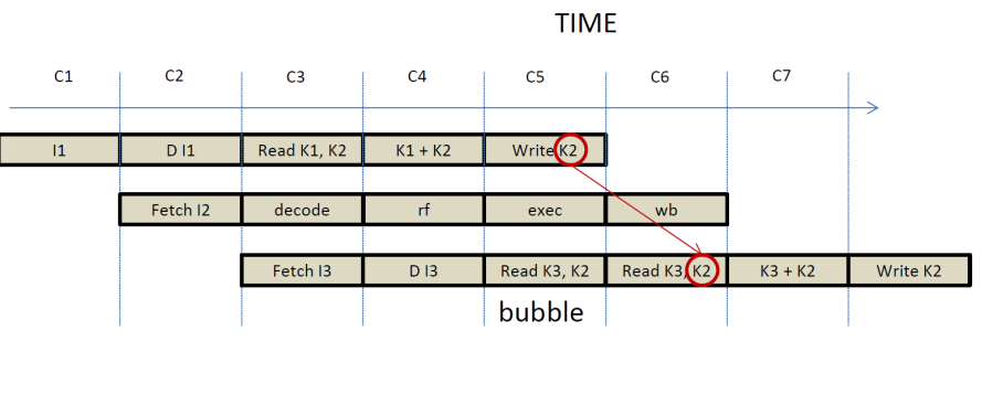
Data Hazards:
Let us consider the
following instruction sequence:
I1: ADD K2 K1
I2: ADD K0 K0
I3: ADD K3 K2
Instruction I1 writes to
register K2 while instruction I3 reads that value. Let’s see how these will
happen in time and whether they will execute correctly on our pipeline:
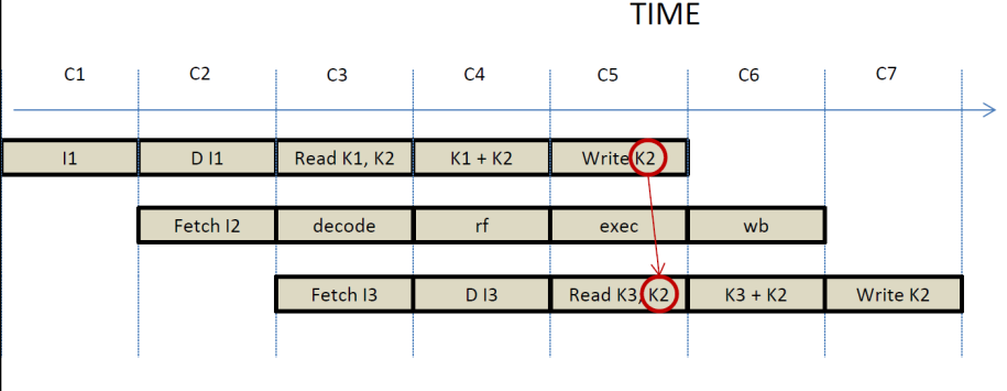
At cycle C5, I1 will
be writing K2, while I3 will be reading K2. If we use edge triggered flip-flops
for the registers, the write of I1 will happen at the end of the clock cycle,
while the read will happen during the clock cycle. As a result I5 will read the
previous value of K2 and not the one I1 is writing. In this case
execution will be incorrect.
There are two
possible solutions to this problem. The first to delay I5 by one cycle
and the second is to bypass or forward the value from ALUout into
R2.
Data Hazards -- Bubbles:
Let’s look at the
first option. The goal here is to delay the execution of I5 by one cycle. The
decision that needs to happen can be taken during the RF stage for I5. At this
stage, the RF stage can compare the destination register of the WB stage with
the source registers being used during the RF stage. If they are the same, then
at the end of the cycle, all stages from RF and earlier that includes
the DECODE and FETCH stages, will be loaded with their current input values.
That is their stage registers will be loaded with the same values as before
through a feedback connection. This is called a pipeline bubble. In time
execution now will proceed as follows:
The control logic of
the RF stage will need to detect whether a bubble is necessary. This can be
done by comparing the register names that it is currently using (found in IR3)
with those written into by the WB stage (found in IR4). If a data hazard is
detected, then the RF stage will have to notify both the DECODE and the FETCH
stage. In general, bubbles affect all preceding stages. If our pipeline has 10
stages and a bubble had to be inserted at stage 5, then all stages from 5 and
below would have to repeat the same action next cycle. That is all stages will
have to reload their input stage registers with their current values and
prevent loading the value from their preceding stage. As we know the FETCH
stage has no input stage register. What needs to be done for it? We can either
inhibit another fetch from memory since the one we just did is good enough, or
we can inhibit the update to the PC. Either solution is fine, the first reduces
energy but may run into problems with self-modifying code. The second solution
where the FETCH repeats the fetch will work no matter what but does use more
energy because it repeats the memory read.
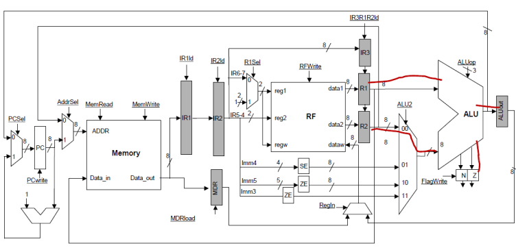
Data Hazards -- Bypass:
As we said, during
the RF stage I3 can detect that is reading is value that will be written into
K2 at the end of the clock cycle. However, that value is currently available as
the output of ALUout (the output register of the EXEC stage). Note that all
that is needed is that the right value gets loaded at the end in register R2
(the output register of the RF stage). Accordingly, we can bypass through a
multiplexer the ALUout value to R2 instead of the value read from the register
file. The modified datapath is as follows:
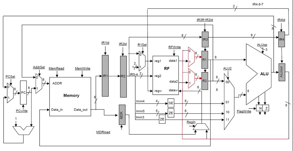
R1 and R2 now are
driven by two multiplexers. Each of those multiplexers can either pass the
value read from the register file, or bypass the value currently in ALUout. The
diagram does not show the control logic needed to make the selection. In our
case, this logic would have to compare the register identifiers fed to the
register file (these are found in IR2) with the destination register of the
instruction in stage WB. This can be found in IR4. If they are the same, the
value can be bypassed.
In our discussion we
have assume that it is not possible to directly bypass the value through the
register file. The reality of custom build register files is such that the
write can happen in the first half of the clock cycle and the read can then
proceed in the second half. If you pick up most books that cover pipelining you
will see this as the base assumption. In such a design, there is no need for an
explicit bypass as this is done internally in the register file assuming that
the registers are latches and not edged triggered. With edge triggered register
elements as the ones we assumed, explicit forwarding paths are necessary.
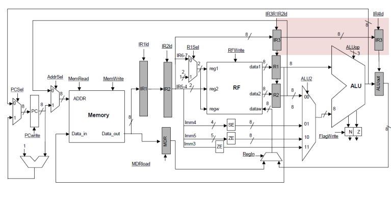
Now let’s consider
the following instruction sequence:
I1: ADD K2 K1
I2: ADD K3 K2
I2 must read the
value for K2 that I1 is producing. In time this will appear as follows:
From this time
diagram it would appear that we have no option other than to delay I2 since the
value it needs to read in stage 3 at cycle C4 does not get written back until
stage 5 of I1 which occurs a cycle later in C5. However, observe the following:
1.
The
value for K2 has been calculated by I1 in C4 and has been stored in ALUout.
2.
The
value for K2 is only needed by I2 in cycle C5 where the actual calculation
takes place.
So, in reality the
data dependency between I2 and I1 appears as follows:
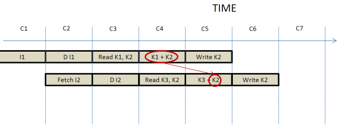
Now the arrow moves forward
in time, which is to say that the value gets produced before it needs to be consumed. To do this, however, we need to
further extend our datapath to allow forwarding from WB to EXEC (before we did
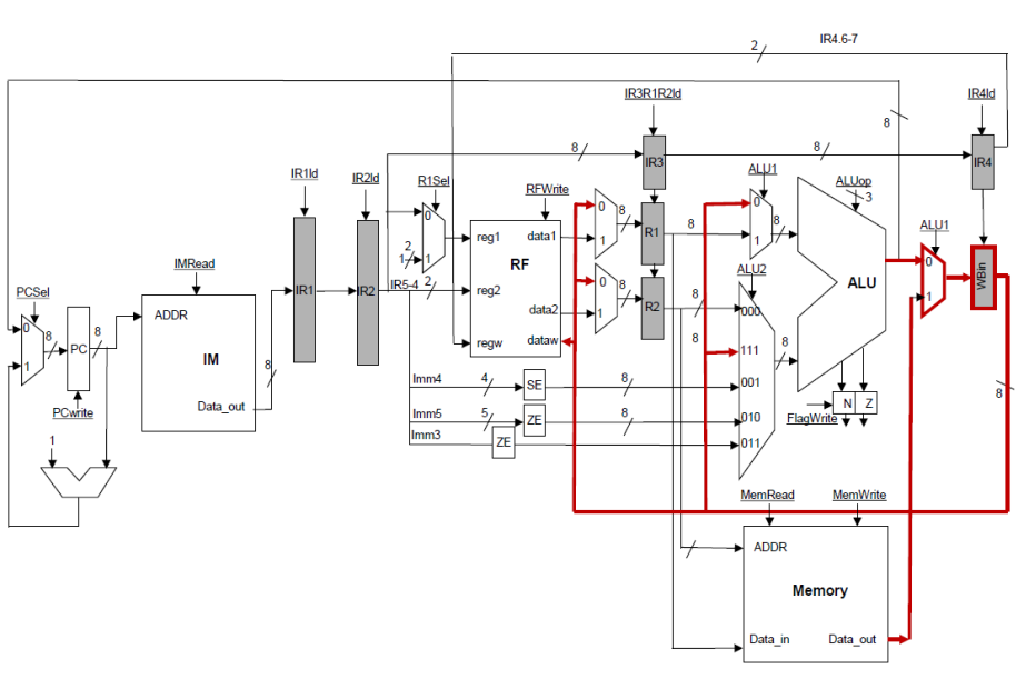
forwarding to WB to RF):
The control logic of
the EXEC stage will have to compare the two source registers (found in the IR3
register) and compare them with the register in the WB stage as found in IR4.
If the names are the same, the value can be bypassed through the ALU1 and or
ALU2 multiplexers.
This concludes the
pipelined design for ADD, SUB and NAND. We next proceed to consider the other
instructions.
ORI and SHIFT:
ORI and SHIFT are
structurally similar to ADD. The difference is that ORI does not provide the
registers as part of the instruction while the second operand for both ORI and
SHIFT comes from the instruction as an Imm5 or Imm3. Our datapath is already
capable of performing those operations. The bypass logic will have to be
modified to take into consideration the instruction opcode to work correctly
for these instructions. It will have to use the name K1 when comparing for
bypassing with the EXEC and WB stages, and use K1 as the destination register
for those stages as well. For shift, it has use only the R1 field from the
instruction since SHIFT does not use a second register operand.
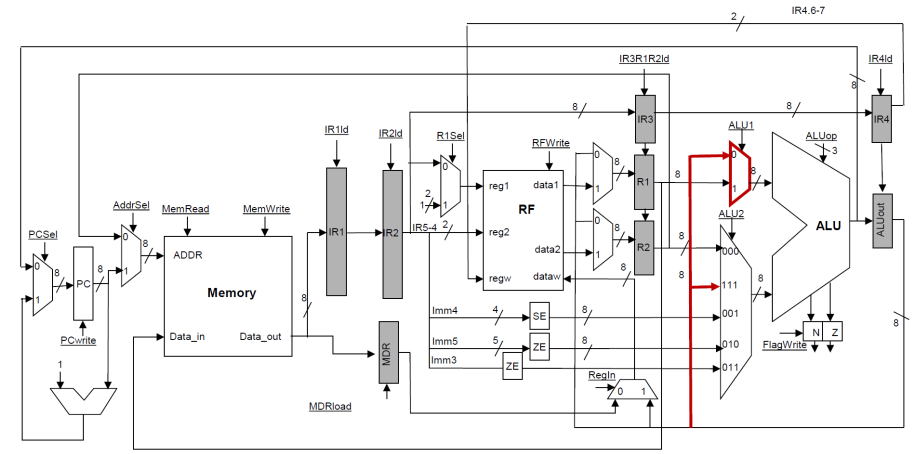
STORE:
The store
instruction is identical to ADD up to and including the RF stage. In the EXEC
stage, however, it needs to write to memory. Unfortunately, memory is already
being used by the FETCH stage of every instruction. So, we have a structural
hazard since all instructions read from memory to fetch during the FETCH
stage and stores also try to write to memory at their fourth stage, the EXEC
stage. How can we overcome this problem? There are two solutions:
1.
Bubble:
Give priority to the store over the instruction currently at FETCH.
2.
Replicate:
Use a second memory for data accesses.
Let’s look at these
options more closely.
Allowing Memory Writes with a single memory:
If we opt for the
bubble approach, we need to prevent the FETCH stage from accessing memory while
a store is at its EXEC stage. In time this will look as follows:
This solution
requires no modification to the datapath. The control of the EXEC stage will
need to detect that it executes a STORE
instruction and accordingly set the MemWrite, and AddrSelect signals. The
control of the FETCH stage will need to inhibit writing to the PC and disable
the MemRead signal. So, the two stages will have to coordinate and moreover,
the decision is best taken by the end of stage RF instead. That is, when a
STORE enters the RF stage, it can signal that in the next cycle FETCH should be
de-activated.
Replicating Memory:
The other solution
is to use a separate memory for instructions and another one for data. This is
a Harvard-style architecture which is familiar to use from the single-cycle
implementation. This is exactly the architecture of choice being used today.
However, instead of having separate instruction and data memories, modern
processors use a unified memory space for both instructions and data.
Pipelining is possible by using separate caches for instructions and
data. Those caches feed from the same memory, however, they can be accessed
independently. As long as the access hits, the pipeline can proceed
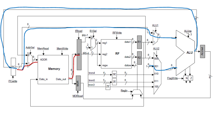
unabated. Here’s the modified datapath:
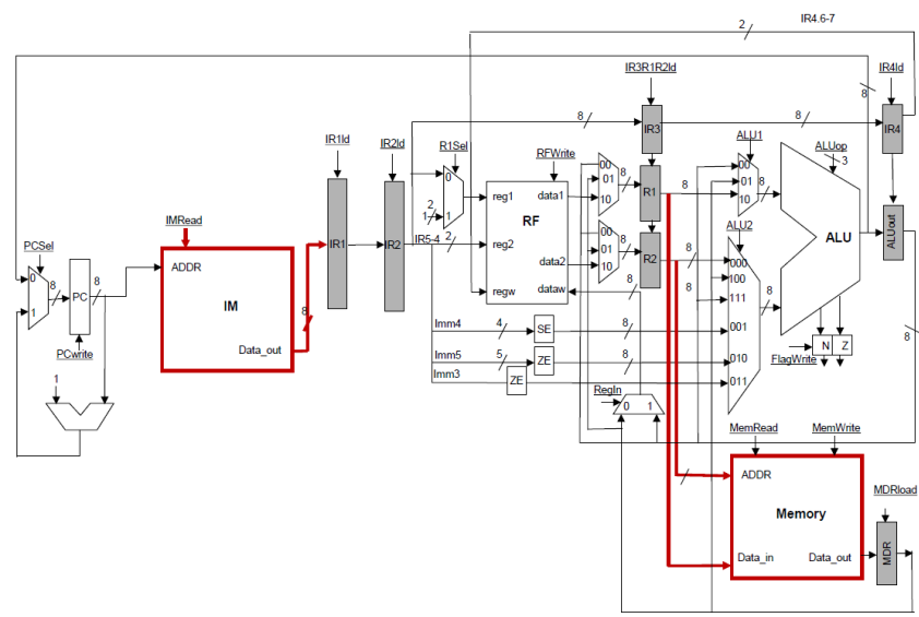
The figure contains
the changes for the LOAD instruction as well which are explained next.
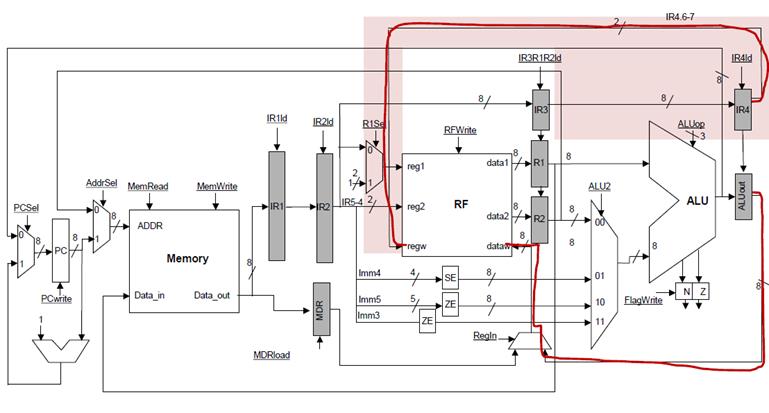
LOAD:
For load we need to
access memory at the EXEC stage, something we’ve already supported as part of
the discussion for STORES. The result of the memory read gets stored in the MDR
register. We then need at the WB stage to write to the RF. The diagram below
shows how this can be done. We need to introduce additional bypass options to
support bypassing MDR from WB to RF and from WB to EXEC:
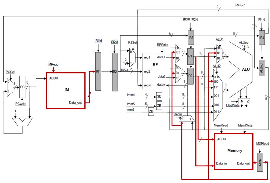
Instead of having
loads and ALU operations write to different registers at the EXEC stage, we can
instead unify ALUout and MDR. The modified datapath now does not need extra
bypass options, moreover, we no longer need a multiplexer to select the value
that will be written into the register file:
Branches:
All instructions we saw
thus far update the PC to be PC + 1. Branches however may further update the
PC. Let’s first look at where the branches may do that update. The information
needed to do that update comprises the following:
1.
Which
branch this instruction is. This is known after DECODE.
2.
What is
the value of the flags. This may be produced as later as the end of EXEC of the
immediately preceding instruction.
Accordingly the
simplest approach is to have branches update the PC during the EXEC stage. The
datapath is as follows:

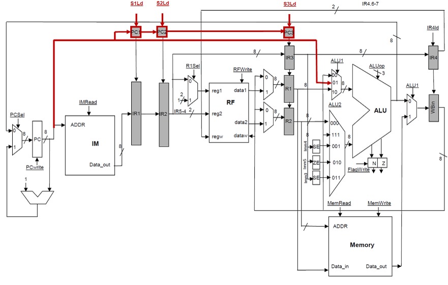
The first input to
the ALU now can also pass the value of PC3. PC1, PC2, and PC3 are pipeline
registers that carry the value PC+1 for the corresponding instruction. When the
branch gets fetched, it also updates the PC to be PC+1. That value gets written
back into the PC and carried with the branch into PC1. As the branch moves from
stage to stage, its PC value flows with it, so that the correct calculation can
take place in the EXEC stage as shown. When a branch executes in the EXEC stage
and is taken, that is it decides to update the PC, all instructions that follow
must be squashed. That is the must be not allowed to make any changed to
architectural state which includes registers, memory, flags and the PC. The
instructions that must be squashed include those in the FETCH, DECODE, and RF
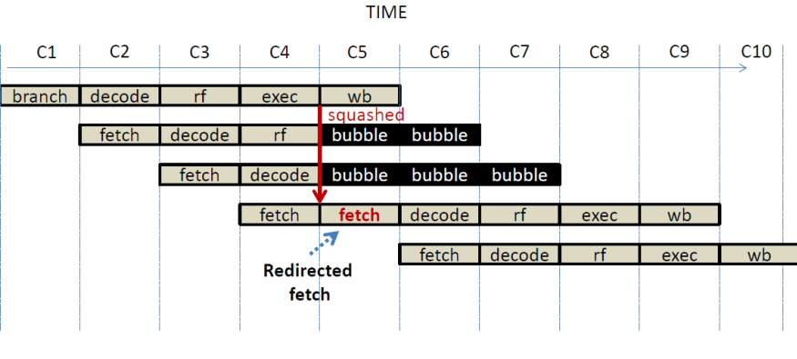
stages. In time execution flows like this:
Control Flow Hazards:
Every branch
instruction creates a control flow dependency for the instructions that
follow it. That is, when we encounter a branch we do not know which instruction
will execute next until we execute the branch to completion. In the pipeline
this manifests as a control flow hazard, or simply a control hazard. The
simplest approach to handling control hazards would be to stall. That is,
whenever a branch is fetched we would stall the pipeline until the branch
executes, or resolves. Unfortunately, we do not know whether the
instruction is a branch until the end of decode. Accordingly the stall approach
would stall the pipeline for a cycle after fetching any instruction to wait to
make sure that the instruction is not a branch. The pipeline we designed thus
far, does not use this approach. Instead it uses control flow speculation. In
control flow speculation the pipeline guesses what is the address of the next instruction to fetch and proceeds to
do so speculatively. Eventually when the instruction is known and
executes, the speculation is validated. If it was correct, no further action is
necessary and we gained performance since we speculatively executed the right
instructions without waiting to make
sure that we should. If however, the speculation is incorrect, we have a misspeculation
and we must:
(1) Undo all speculative changes done by the incorrectly executed
instructions
(2) Redirect fetch to the right instruction.
Let’s see now how
these concepts apply to our pipeline.
To do control flow
speculation or branch speculation we first need a branch predictor. A
branch predictor does two things:
1.
Speculate
whether the branch is taken or not. This is a binary decision.
2.
Speculate
what is the exact address of the next instruction.
Our pipeline uses a
simple, static branch predictor that speculates always not taken.
So, it always answer Q1 above with not taken. For Q2 it does not need to
speculate since we already have the PC and can calculate the fall through PC as
PC +1. This is a static branch predictor since its decision does not get
influenced by program execution. No matter what it is always the same.
In the event of
misspeculation we need to first undo any speculative changes and then redirect
fetch. Let’s look at where changes to architectural state happen:
1.
All
instructions update the PC with PC+1 at FETCH.
2.
Some
instructions update the flags in EXEC.
3.
Stores
update memory in EXEC.
4.
ADD,
SUB, NAND, ORI, SHIFT, and LOAD, update the registers at WB.
Branches signal a
misspeculation at the end of their EXEC stage. Instructions that follow the
branch appear at earlier stages and they had no chance of updating any
architectural state except for the PC. As we have seen the branch carries the
PC with it, and calculates the right target at EXEC. Accordingly, the PC gets
correctly updated on a misspeculation.
As a result, our pipelined implementation correctly handles branch
mispeculations.
Summary of what happens when:
The following table
summarizes what each instruction does at each stage.
|
CYCLE |
|
Instruction Class |
|||||||
|
|
|
ADD, SUB, NAND |
SHIFT |
ORI |
LOAD |
STORE |
BPZ |
BZ |
BNZ |
|
1 |
FETCH |
[IR] = Mem[ [PC] ] [PC] = [PC] + 1 |
|||||||
|
2 |
DECODE |
||||||||
|
3 |
RF |
[R1] = RF[ [IR7..6] ] [R2] = RF[ [IR5..4] ] |
[R1] = RF [1] |
[R1] = RF[ [IR7..6] ] [R2] = RF[ [IR5..4] ] |
|
|
|
||
|
4 |
EXECUTE |
[WBin] = [R1] op [R2] |
[WBin] = [R1] shift Imm3 |
[WBin] = [R1] OR Imm5 |
[WBin] = Mem[ [R2] ] |
MEM[[R2] = [R1] |
if (N’) PC = PC + SE(Imm4) |
if (Z) PC = PC + SE(Imm4) |
if (‘Z) PC = PC + SE(Imm4) |
|
5 |
WRITEBACK |
RF[[IR7..6]] = [WBin] |
RF[ 1 ] = [WBin] |
RF[[IR7..6]] = [WBin] |
|
|
|
|
|
Adhering to Sequential Semantics:
Early on in the
lectures, we discussed that conventional programs use sequential semantics. That
is, instructions are supposed to execute one after the other in order and
without any overlap. Pipelining, however, allows the partial overlap of
instructions. Does our pipelined implementation still adhere to sequential
semantics? To reason about this let’s try to better understand what sequential
semantics really calls for. An equivalent definition would be that at any given
point in time, if one stops and inspects the architectural state, it should be
such that:
1.
All
instructions in the original sequential execution order up to and including
some instruction A have executed. That is they have made all their changes to
the architectural state.
2.
No
instruction after A has made any changes to the architectural state.
For example, assume
a sequence of instructions A, B, C, D, and so on, as they would have executed
sequentially. If we stop the processor at any point and inspect its
architectural state (that is registers, PC, memory and flags), the above two
conditions must hold. That is if C has executed, the A and B must have executed
too, and no changes from D, or E and so on should be visible. Equivalent, if we
take an execution timeline in the pipeline, we should always be able to draw a
vertical line such that all instructions before it made all their changes to
the architectural state and no instruction after it has made any changes:
Let us focus on the
point in time A. At this point, the first instruction has just finished the
EXEC stage. If this is an ADD it could have updated the flags. Say that is an
ADD K2 K1. If the machine is stopped at this point, an outside observer could
see that the flags have been updated but the register file for K1 has not. As a
result, this implementation would violate sequential semantics. However, recall
that they only way someone could observe the register values would be by
executing an instruction that reads them. So, the observer would try to read K2
through an instruction that possibly follows immediately our ADD. Our pipeline
has bypass paths that would correctly bypass the value from WB to EXEC or RF,
accordingly, to the outside observer it would as if the register has been
updated at the same time as the flags. Hence our pipelined implementation would
appear to be adhering to sequential execution semantics.
Similar reasoning
applies to STORES that update memory in the EXEC stage. The only instructions
that can observe the change are LOADS which also access memory at the EXEC
stage. Moreover, changes to the registers are visible to other instructions
immediately after the EXEC stage. So, to an outside observer all architectural
state changes appear to happen at the end of the EXEC stage or equivalently the
beginning of the WB stage. The only exception is the PC which gets updated at
the FETCH stage. If it was possible to read the PC value once could detect
those changes. There is no instruction in our architecture that reads the PC as
data. Accordingly, it is not possible to directly observe the value of the PC.
However, even if it was, recall that our instructions carry their PC value
along with them in registers PC1, PC2, PC3 as they pass through the pipeline
stages. Accordingly, the PC could be
treated like any other register and bypassed accordingly similarly to what we
did for the K registers at the EXEC and WB stages.
For registers, flags
and memory all updates become visible at the EXEC stage. For PC we can
introduce bypassing to maintain the illusion of sequential execution as needed.