ECE1388: VLSI Design Methodology
A 6-bit Flash ADC in 0.35 um CMOS
David Alldred
Overview
The project consisted of the schematic design and layout of a 6-bit ADC in 0.35 um CMOS using a Flash architecture. It employs inverter-threshold comparators, discussed in [1], which dissipate no static power and do not require a voltage reference or clock. Due to the long settling time of the comparators, a track and hold was utilized at the input to achieve large bandwidth with sufficient accuracy. The digital thermometer code outputs are encoded first into one-hot and then into the binary output bits. A block diagram of the ADC is shown in Figure A.1.
Specifications
The settling time of the comparators, upwards of 2 ns for inputs close to the threshold, limited the sampling rate limited to a maximum of 500 MS/s. The track and hold has a large bandwidth so sampling of inputs signals beyond Nyquist (up to almost 1 GHz) should be possible. The input voltage range is 1.1 Vp-p with a common-mode of 0.55 V. The entire ADC dissipates 61.8 mA from a two separate, analog and digital, 3.3 V supplies for a power consumption of 204 mW. A transient simulation verifying correct operation at 500 MS/s with a ramp input is shown in Figure D.1.
Block Design
Analog
Track and Hold
The track and hold circuit, adapted from [2], employs two source-follower circuits as shown in the schematic of Figure B.1. The first one maintains a constant gate-source voltage across the switch during the sample phase such that signal-dependent charge-injection errors are reduced. The second buffers the sampling capacitor voltage so that it is not affected by the comparators. The circuit consumes 37 mA and is the only source of static power consumption in the ADC. The layout of the track and hold is shown in Figure C.1.
Comparators
The inverter-threshold comparator thresholds are determined by the W/L ratio of the first inverter shown in the schematic of Figure B.2. The NMOS is fixed at 3.2 um while the PMOS widths range from 3.2 um to 64 um. The minimum length is required to limit INL/DNL error due to the minimum grid resolution (0.025 um) to around 0.05/0.1 LSB. Figure D.2 shows the INL/DNL for the comparators, which is worst for the smaller comparators as expected. The maximum length was determined by the desired input signal swing of at least 1 V. Two additional inverters are added to increase the gain of the comparators. The layout of the entire bank of comparators is shown in Figure C.2.
Digital
Registers
The registers are implemented using a standard master-slave flip-flop from Weste as shown in Figure B.3. The layout of this cell, shown in Figure C.3, set the pitch of the 63-bit datapath to 7.5 um.
Thermometer to One-Hot Encoder
A set of simple 3-input NAND gates as shown in Figure B.4 was used to implement this encoder. By looking at the codes one and two levels above the encoded bit it can prevent single bubble errors. The encoded bit with the inverter was connected to the top input of the NAND gate since it is the fastest. Much effort was put into fitting the layout of the unit cell, shown in Figure C.4, into the 7.5 um pitch set by the flip-flops.
One-Hot to Binary Encoder
This encoder was implemented using 6 32-input dynamic OR gates for which the schematic is shown in Figure B.5. During one half of the clock cycle the bit line in each DOR is precharged high and during the other half they are possibly pulled low depending on the output code. An inverter at the output generates the proper polarity. The layout of the entire encoder is found in Figure C.5.
Output Registers and Buffers
A set of six registers are used to store the output code which is available 2 clock cycles after it was sampled at the input on a falling clock edge. A differential clock is also buffered to output pads to facilitate easier recovery of the (up to 500 MHz) data outside the chip, for a total of eight output buffers.
Clock Management
This block generates differential clocks with enough drive strength to operate all of the blocks in the chip. The fan-out of each inverter was kept between approximately 1.5 (for the T/H) and 2.5 to ensure that the clock edges were sharp and avoid excessive switching times. The schematic, including details regarding the fan-out of each stage, is found in Figure B.6.
Chip Layout
The major blocks were assembled according to the floor plan of Figure A.2 to form the core of the ADC, whose layout is shown in Figure C.6. A guard ring was added around the analog blocks to protect them from substrate noise generated by the digital blocks. The pad frame and pin arrangement was planned according to Figure A.3. It can be seen that the chip was core-limited in area. Once the pad frame was built a power grid was constructed to provide power to the core using M4. The layout of the pad frame including the power grid is found in Figure C.7. The final chip layout is 0.73 mm x 0.55 mm including the pad frame for a total area of 0.4 mm2 and is shown in Figure C.8. The final layout is DRC and LVS clean and the LVS report can be found in Appendix E. A summary of the pin-out is shown in Table 1 below.
|
Pin Name |
Type |
Description |
|
Vdd |
Digital Power |
3.3 V Supply |
|
Vdda |
Analog Power |
3.3 V Supply |
|
Vss |
Analog/Digital Power |
Common Ground |
|
IN |
Analog Input |
Signal Input |
|
Vb |
Analog Bias |
T/H Bias Voltage |
|
CLK |
Digital Input |
ADC Clock Input |
|
D<5:0> |
Digital Output |
Output Code |
|
CLKP/N |
Digital Output |
Output Clock |
Table 1: Pin-out Descriptions
References
[1] J. Yoo, K. Choi, A. Tangel, “A 1 GSPS CMOS Flash A/D Converter for SOC Applications,” Proceedings of IEEE Computer Society Worskhop on VLSI 2000, pp. 135-139, 2001.
[2] D. Jakonis, C. Svensson, “A 1 GHz Linearized CMOS Track-and-Hold Circuit,” Proceedings of the IEEE ISCAS, vol. II, 2002.
Appendix A – Block Diagram and Floor Plans
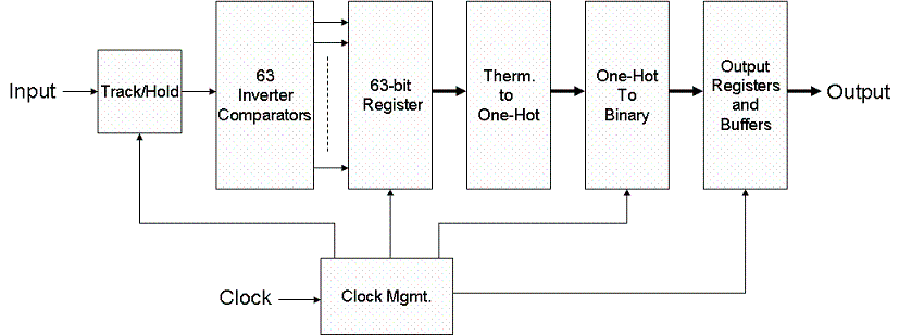
Figure A.1: ADC Block Diagram
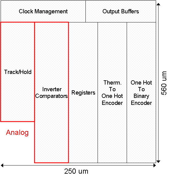
Figure A.2: ADC Core Floor Plan
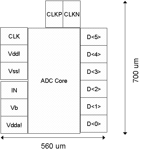
Figure A.3: Pad Ring Floor Plan
Appendix B – Block Schematics
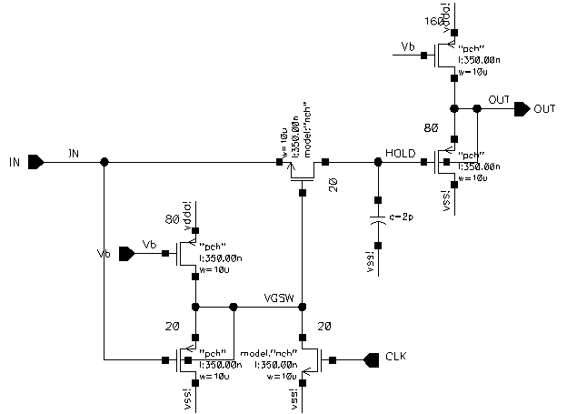
Figure B.1: Track and Hold Schematic
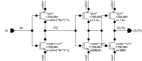
Figure B.2: Inverter-Threshold Comparator Schematic
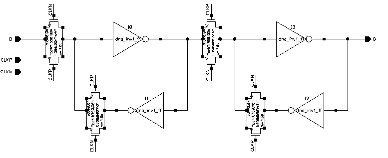
Figure B.3: Flip-flop Register Schematic
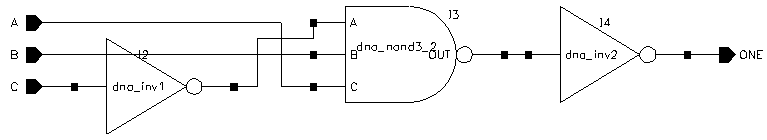
Figure B.4: Thermometer to One-Hot Encoder Unit Schematic
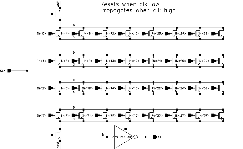
Figure B.5: 32-Input Dynamic OR Gate Schematic
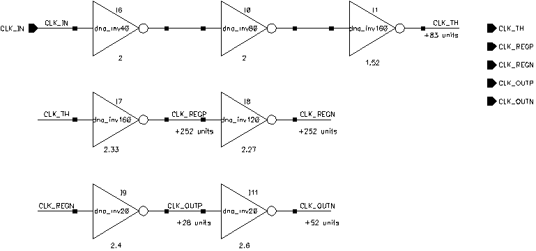
Figure B.6: Clock Management Schematic
Appendix C – Layouts
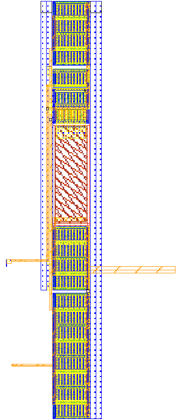
Figure C.1: Track and Hold Layout
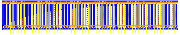
Figure C.2: I-T Comparator Bank Layout
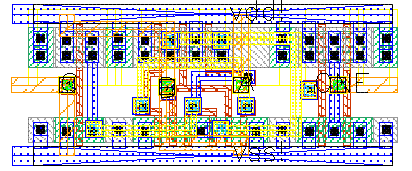
Figure C.3:Flip-flop Register Layout
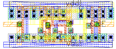
Figure C.4: Thermometer to One-Hot Encoder Unit Layout
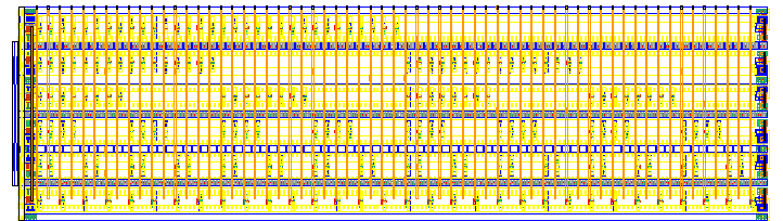
Figure C.5: One-hot to Binary Encoder Layout (stretched to show detail)
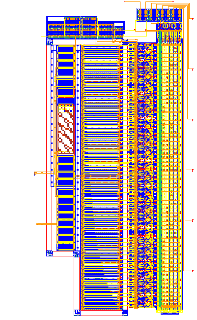
Figure C.6: ADC Core Layout
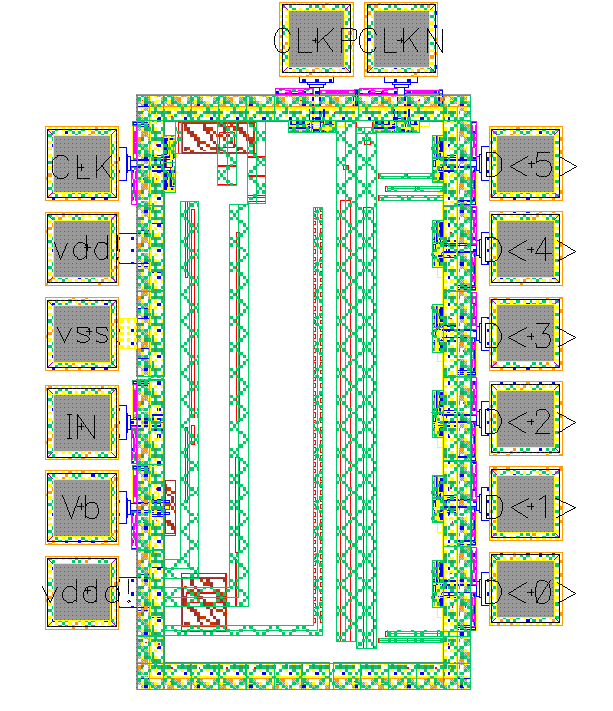
Figure C.7: Pad Ring and Power Grid Layout
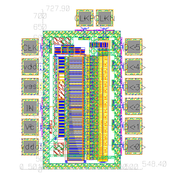
Figure C.8: Final Top-Level Layout
Appendix D – Simulation Results
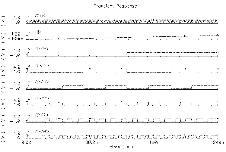
Figure D.1: Transient Simulation with Ramp Input at 500 MS/s
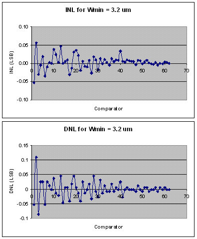
Figure D.2: INL and DNL Error due to Comparators
Appendix E – Chip LVS Report
@(#)$CDS: LVS version 5.0.0
08/17/2004 10:15 (cds12107) $
Command line: /nfs/vrg/cmc/cmc/tools/cadence.2003a/IC5033USR3/tools.sun4v/dfII/bin/32bit/LVS
-dir /johns/b/b1/alldred/1388/cmosp35/LVS -l -s -f -t
/johns/b/b1/alldred/1388/cmosp35/LVS/layout
/johns/b/b1/alldred/1388/cmosp35/LVS/schematic
Like matching is enabled.
Net swapping is enabled.
Fixed device checking is
enabled.
Using
terminal names as correspondence points.
Net-list summary for
/johns/b/b1/alldred/1388/cmosp35/LVS/layout/netlist
count
1112 nets
14 terminals
2002 nfet
22 diode
4 capacitor
1939 pfet
Net-list summary for
/johns/b/b1/alldred/1388/cmosp35/LVS/schematic/netlist
count
1112 nets
14 terminals
1964 nfet
22 diode
4 capacitor
1603 pfet
Terminal correspondence points
N612
N17 CLK
N485
N11 CLKN
N1113
N10 CLKP
N7
N14 D<0>
N209
N21 D<1>
N821
N3 D<2>
N618
N23 D<3>
N1255
N12 D<4>
N271
N15 D<5>
N1316
N24 IN
N387
N18 Vb
N680
N0 vdd!
N279
N2 vdda!
N624
N1 vss!
126 net-list ambiguities
were resolved by random selection.
The net-lists match.
layout schematic
instances
un-matched 0 0
rewired 0 0
size errors 0 0
pruned 0 0
active 3967 3593
total 3967 3593
nets
un-matched 0 0
merged 0 0
pruned 0 0
active 1112 1112
total 1112 1112
terminals
un-matched 0 0
matched but
different type 0 0
total 14 14
Probe files from
/johns/b/b1/alldred/1388/cmosp35/LVS/schematic
devbad.out:
netbad.out:
mergenet.out:
termbad.out:
prunenet.out:
prunedev.out:
audit.out:
Probe files from
/johns/b/b1/alldred/1388/cmosp35/LVS/layout
devbad.out:
netbad.out:
mergenet.out:
termbad.out:
prunenet.out:
prunedev.out:
audit.out: