
ECE1388 Final Project
openMSP430 Implementation-Dual Slope ADC
ECE1388 VLSI Design Methodology - Final Project Report
openMSP430 VLSI Implementation and Dual Slope ADC design
Team Members:
Jaimin Joshi – M.Eng Electronics
1003594014
Jialing Wang – M.Eng Electronics
1002908302
Srinidhi Balasubrahmanya – M.Eng Electronics
1003072435
University of Toronto
19 th Dec 2016
1

ECE1388 Final Project
openMSP430 Implementation-Dual Slope ADC
The aim of this project was to implement the openMSP430 open source microcontroller core in VLSI architecture, in
conjunction with an Analog to Digital converter (ADC). The motivation behind this project is the recent emergence and
growing trend of the ‘Internet of Things’ (IoT) industry [7] . Incorporating an ADC with a microcontroller provides a medium
to interact with the physical environment and connect objects to each other. If the project were to be expanded and
wireless capabilities were added, the chip could be used for IoT applications.
As highlighted in Table 1, the main advantage of using MSP430 architecture as opposed to other microcontrollers such
as PIC16F877A or Atmel ATMEGA328 is the fact that the MSP430 provides greater accuracy due to its 16-bit CPU and
consumes the lowest power (0.23mA), making it ideal for VLSI implementation.
The ADC designed in this project was to be used for low frequency and high accuracy applications such as temperature
sensing. From Table 2 it can be seen that the dual slope ADC is ideal for this application as it has low speed power
consumption with high accuracy. Unlike a single slope ADC’s, the accuracy of a dual slope ADC does not depend on
the RC components, providing greater accuracy.
Design of Dual Slope ADC :
The operation of the Dual Slope ADC can be segmented into two components, one that deals with Analog input and the
other which deals with conversion to Digital. The Analog design is responsible for converting Voltage to Time domain
in a way that the Time converted is proportional to the Input voltage. The Digital component is responsible to count this
time and storing the output as a converted digital equivalent, until next iteration. The storing is a necessity, since the
counting resets immediately for the next conversion.
As mentioned earlier, the considered ADC converts the voltage to time using capacitor charging and discharging curves.
An op-amp based integrator is therefore required to convert the analog samples of data into time domain by charging
and discharging the capacitor in integrator. The ‘Dual Slope’ nature is implied by the charging of capacitor based on
input voltage value, and the discharge based on a constant voltage (eg. GND as the reference). A comparator is also
required to detect the discharge of the capacitor, which would effectively represent the completion of conversion.
In order to quantize the time domain before the amplitude can be quantized, a sample and hold circuit is required. Since
the Sample-Hold provides the continuous amplitudes for the integrator, we need additional circuitry to provide the ground
voltage reference. An analog switch/mux was designed to intelligently switch between sampled-held signal for the
charge cycle and ground signal for the discharge cycle.
It is clear that if an Op-Amp based integrator is used (which was configured in negative feedback for stability purposes),
an analog voltage inverter is necessary in order to provide the inverted input voltage to the Integrator. An Op-Amp
based Inverting Amplifier was therefore used.
The design considerations of Sample-Hold and Comparator can be realized efficiently using Op-Amp as the base
component. Op-Amp (very high DC gain), in open loop mode, forms an unstable vibrator. This can be exploited to build
the comparator. Ideally an Op-Amp would also have infinite input impedance (very high impedance could practically be
achieved, in range of few G97 which could be exploited to realize the Sample Hold circuit to make sure the sampled
values don’t affect the Input voltage.
Consequently, it was decided to build an effective Op-Amp and utilize it for every component that could be realized
using the same.
The operation can briefly be described as follows:
1. Charge the capacitor (integrate the sampled voltage) with a slope proportional to the input voltage for a
fixed time (say T1)
2. Discharge the capacitor (perform integration using 0V as reference) at constant slope for a time which is
proportional to input voltage say (T2 1 , T2 2 , T2 3 ) for every input voltage which is different than the other.
Op-Amp requirements : DC Gain ~ 1000 (60 dB), Gain Bandwidth ~ 30 MHz, Phase Margin >= 60º, Slew Rate =
20V/µs, ICMR+ = 3.0 V, ICMR- = 1 V, load capacitance C L = 10 pF (assumed for better performance) V DD = 3.3 V,
channel length = 360 nm (assumed for all the FETs).
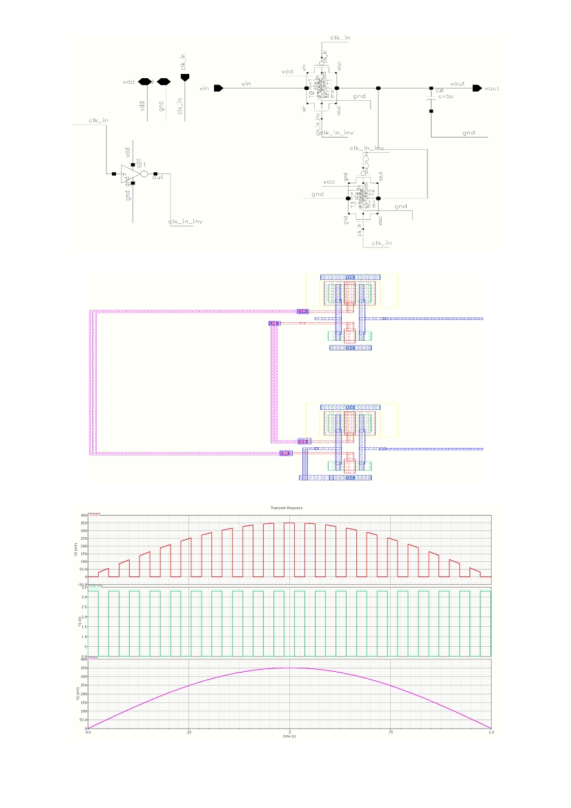
Integrator : An integrator is designed as a negative capacitive feedback of an op-amp as shown in Figure 23 . The
input should always be fed into the inverting input of the op-amp in order to realize a stable (negative feedback) output.
The design considerations of R and C values observed in the Integrator designed is based on the gain required at the
output, considering the pulse width of the input.
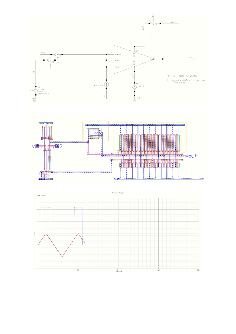
Comparator : A comparator is realized as an open-loop op-amp. Since the op-amp is designed to have very high open
loop DC Gain, the characteristic is exploited to design it as an open loop unstable vibrator when input is fed on non-
2

ECE1388 Final Project
openMSP430 Implementation-Dual Slope ADC
inverting terminal, which either saturates to +VDD (subscript), or to GND, depending on the voltage at the inverting
terminal. Once the voltage at the non-inverting input terminal exceeds the inverting terminal input, the output saturates
to +VDD, and falls to GND when it is lesser. The schematic is shown in Figure 27 .
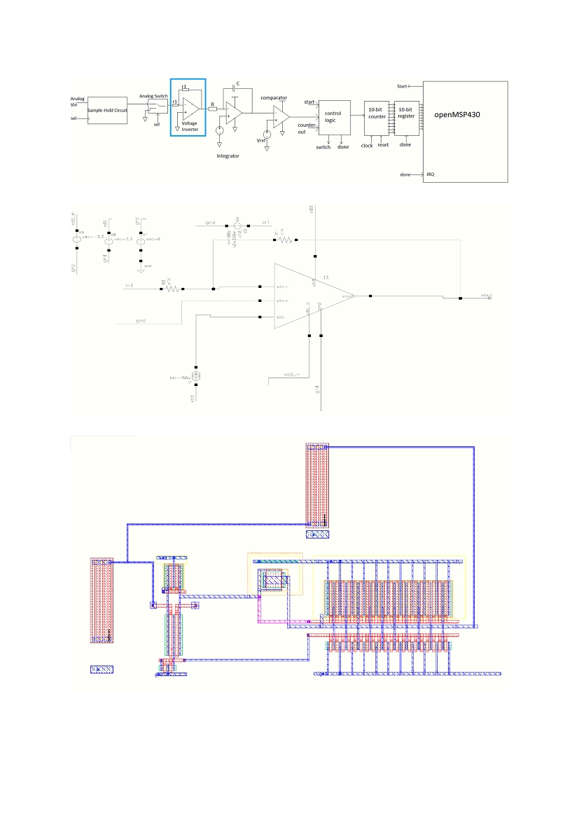
Analog Inverter : As discussed earlier, the input to the integrator should be applied on the inverting terminal; the output
is the inverted integral of the input. To avoid negative integration, we invert the analog input (same magnitude, negative
voltage) to keep the integrator functional and comparator unchanged. It is realized as an op-amp Inverting Amplifier with
gain = -1. Refer to figure Figure 31 for the schematic.
Sample and Hold : Sample - Hold is realized as a two-stage op-amp based capacitive load circuit, where the capacitor
holds the charge, creating a voltage that is equal to the one at the sampling instant. Sampling instants are achieved by
a clock signal arriving from the Control Module (Digital component of ADC). A sampled signal is held for a period 2.56
milliseconds (512 counts on Control Module) which achieves charging of capacitor, plus the duration for which there is
a discharge. The next clock input would be at the instant the discharge is complete, which starts the next sampling
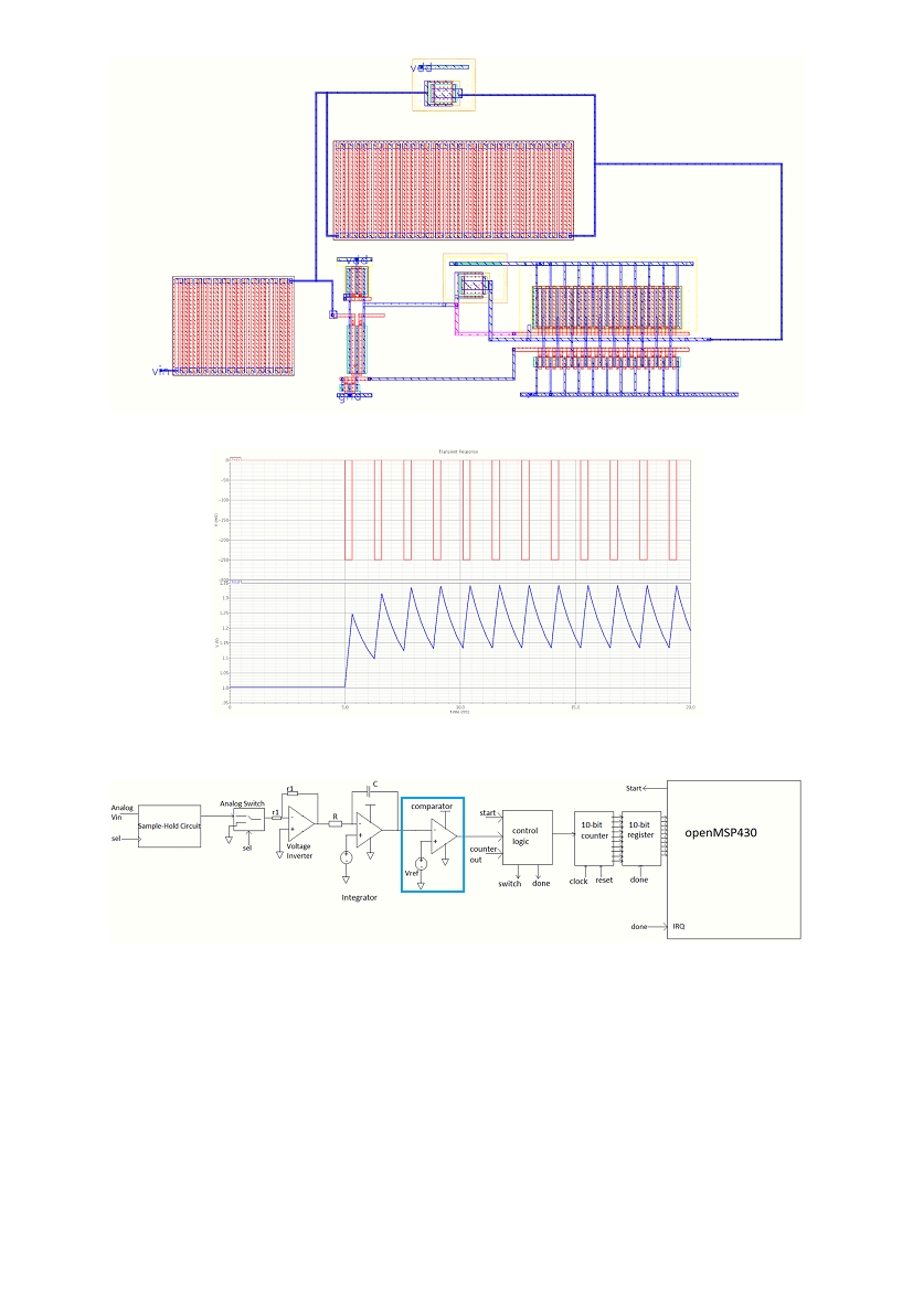
process. Figure 35 represents the Sample - Hold circuit.
Transmission Gate - Analog Switch (MUX): A transmission gate based switch is realized to switch the input to the
integrator between the sampled-held voltage and the ground for a cycle of charging and discharging. The switching
signal is obtained from the Control Module. Refer to Figure 39 for the circuit of the Transmission Gate based Switch.
ADC Specifications
Frequency of operation ~ 200kHz, 10-bit resolution, 61dB SNR, Input voltage range = 1V – 3V
Digital Logic
The digital logic of the ADC consists of the controller, 10-bit register and 10-bit counter. It allows the integrator to
integrate for 512 clock cycles when a full-scale input is applied, which is determined by detecting the instance at which
MSB of the counter is set. Each clock cycle lasts 5µs, hence a frequency of 200kHz and an entire charge cycle could
therefore last a maximum time of 2.56ms. Once 512 clock cycles have elapsed, the controller switches the input of the
integrator to the ground voltage and the capacitor is allowed to discharge. The controller simultaneously resets the
counter. Once a rising pulse is received from the comparator, indicating that the output voltage has fallen below the
reference voltage, the controller sets the ‘done’ signal high, indicating the 10-bit register to store the current value in the
counter. This value can then be used and processed by the microcontroller ALU to calculate the temperature. As the
chip incorporates 8 ADC’s a 10-input multiplexer is used to input the various 10-bit values from all ADC’s to the
microcontroller.
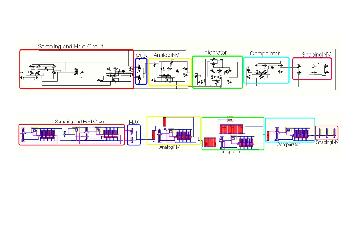
Layout
The layout and schematic of every module labeled in Figure 14 are shown from Figure 18 to Figure 40 . ‘Ncap’ was
chosen as capacitor in the layout as its accuracy of modeling as capacitor is better compared to other components.
Consequently, ‘silres’ was chosen as the resistor due to the same reason. Different widths were set for these
components in order to approach the value of the comparator and resistor in the schematic.
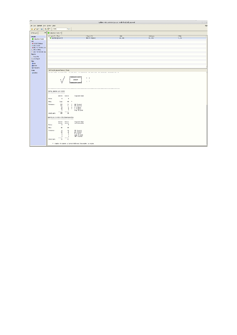
The top level LVS of the analog design of ADC passed successfully in Cadence Virtuoso whilst the Digital design was
verified in Cadence Encounter. The two components were then treated as separate functional blocks and connected in
the pad frame. Due to the dense nature of the imported openMSP430 layout and absence of standard cell layouts in
the IBM 0.13µm technology, rough connections have been made to the control logic using the metals available whilst
connections from the control logic to the microcontroller have been omitted. However, in other kits, the control logic
outputs would connect to IRQ(interrupt) inputs of the microcontroller. The verification reports of the Analog and Digital
blocks have been attached to this report.
openMSP430 Synthesis, Place & Route
Whilst the majority of this project focused on the design of the ADC, the structure of the openMSP430 open core was
observed and understood in order to simulate various segments of the microcontroller and synthesize the design.
Finally, the core was placed and routed in Cadence Encounter. The main exercise in this task was compiling each test
using GCC compiler and use the .mem file generated to simulate the test. Due to the absence of msp-gcc compiler in
Linux environment, the top-level simulation could not be run. Mem file for each test had to be generated on windows
machines and transferred to Linux environment. The openMSP430 manual [4] informed the team about the structure of
complex digital designs and how they can be verified, simulated and synthesized. Further information about the core
can be found in this manual. The stream and netlist files exported from Encounter to Cadence were used to derive the
schematic and layout respectively.
3

ECE1388 Final Project
openMSP430 Implementation-Dual Slope ADC
MSP430
PIC 16F877A
Atmel ATMEGA328
Architecture
MSP
PIC
AVR
Program Memory
32kB
14kB
32kB
CPU
16-bit
8-bit
8-bit
Communication
UART/I2C/SPI
UART/SPI/I2C
UART/SPI/I2C
Protocols
Power Consumption
0.23mA active
0.6mA active
0.2mA active
Table 1. Comparison of (open)MSP430 with other microcontrollers. Source: Atmel[1][2], Circuits Today[3], Microchip[6], Texas Instruments[8]
ADC Type
Speed
Power
Accuracy
Dissipation
Flash
High
High
Low
SAR
Moderate
Medium
Medium
Single Slope
Low
Low
Medium
Dual Slope
Low
Low
High
Sigma-Delta
Low
Low
High
Table 2. Comparison of different types of ADCs. Source: Maxim Integrated[5]
4
ECE1388 Final Project
openMSP430 Implementation-Dual Slope ADC
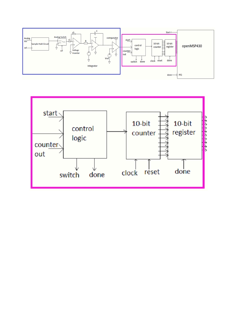
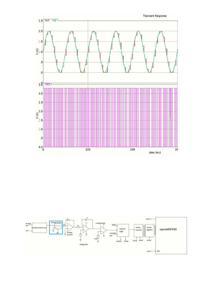
Block Diagram of the System:
Figure 1. Block Diagram of the entire system proposed
Digital Component of ADC (as highlighted in Magenta in Figure 1)
Figure 2. Block Diagram Highlighting the Digital Part of ADC
5
ECE1388 Final Project
openMSP430 Implementation-Dual Slope ADC
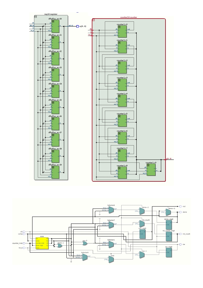
Figure 3. Quartus RTL view of 10-bit counter and register
Figure 4. Quartus RTL view of Controller
6
ECE1388 Final Project
openMSP430 Implementation-Dual Slope ADC
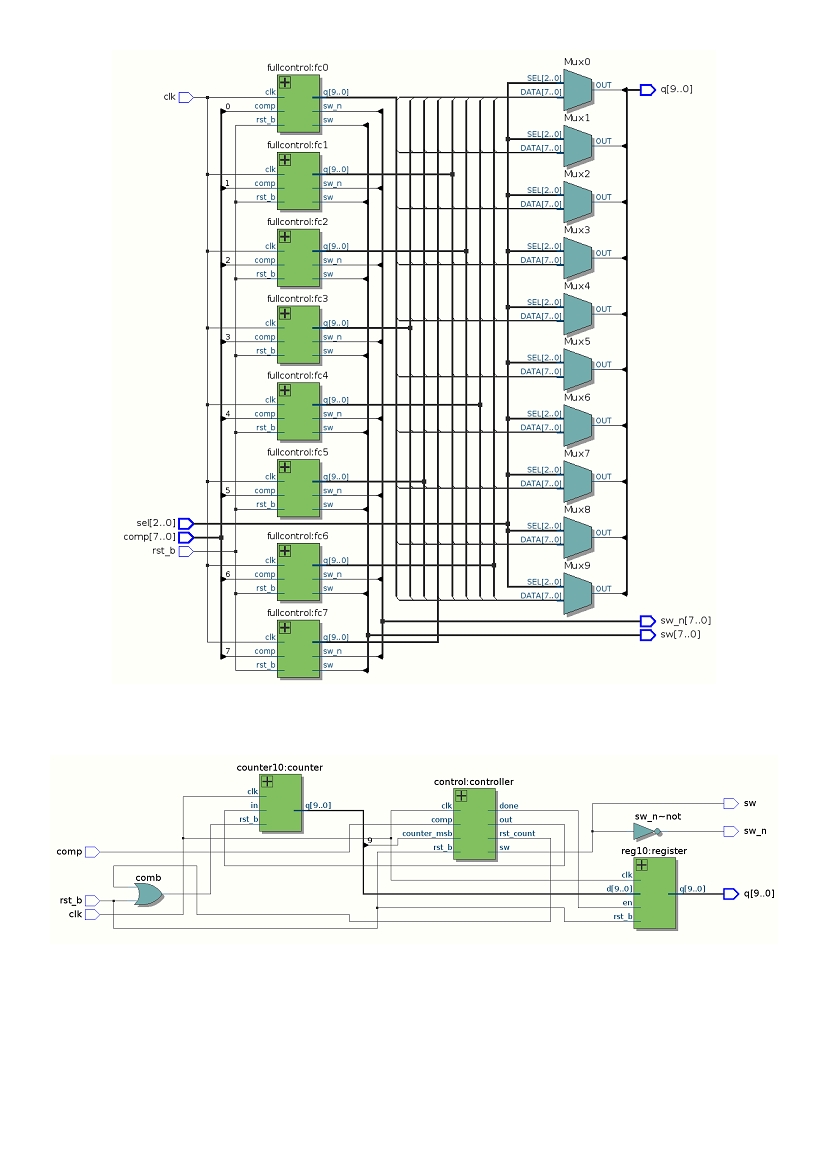
Figure 5. Quartus RTL view of multiplexed control logics
Figure 6. Quartus RTL view of entire control logic
7
ECE1388 Final Project
openMSP430 Implementation-Dual Slope ADC
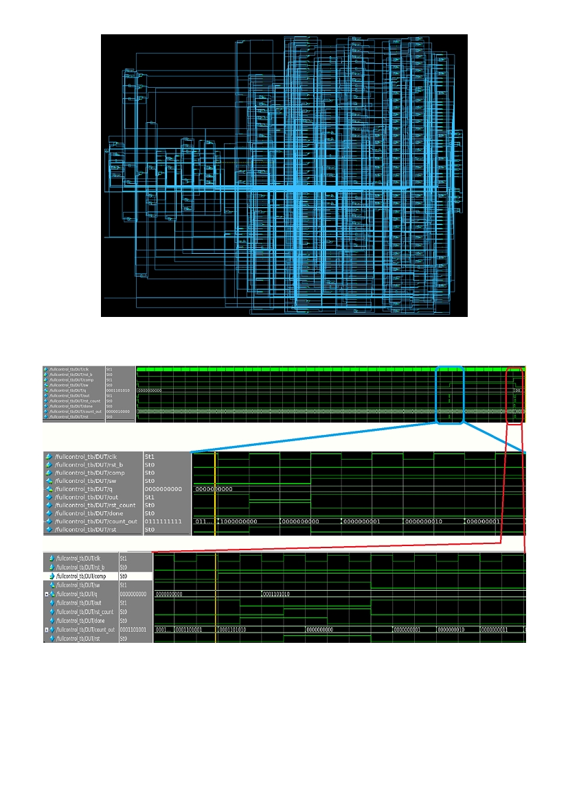
Figure 7. Schematic of all multiplexed control logics imported into Cadence Analog Artist from netlist of the design
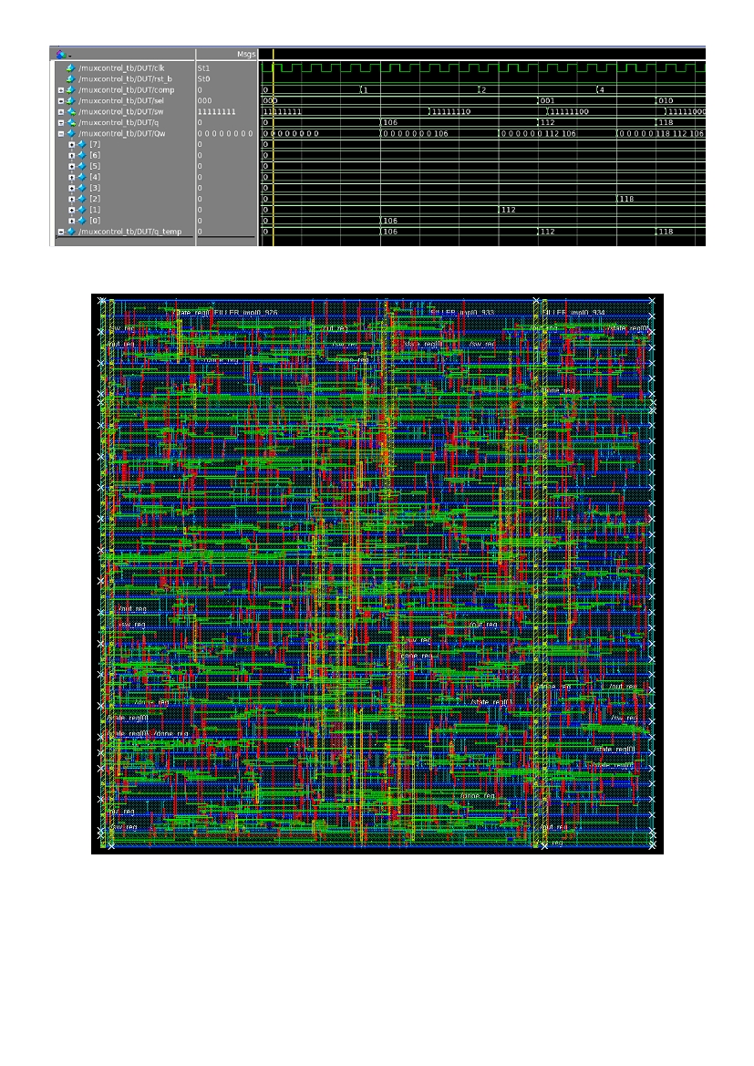
Figure 8. Simulation of control logic indicating switch signal being triggered after 512 clock cycles and done signal triggered after
comparator output detected
8
ECE1388 Final Project
openMSP430 Implementation-Dual Slope ADC
Figure 9. Multiplexer output changing according to select value, based on which comparator output is detected
Figure 10. Placed and routed design of the eight multiplexed control logic units
9
ECE1388 Final Project
openMSP430 Implementation-Dual Slope ADC
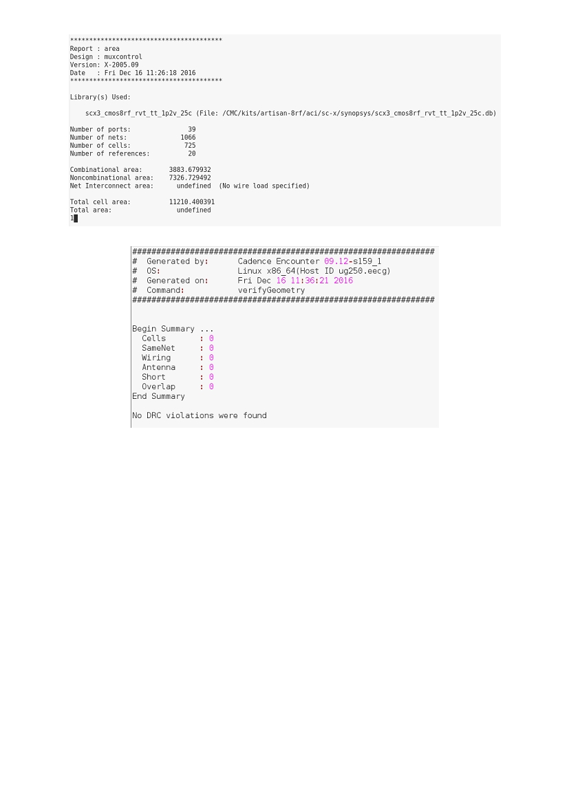
Figure 11. Multiplexed control logic area report
Figure 12. No geometry errors in multiplexed control logic design
10
ECE1388 Final Project
openMSP430 Implementation-Dual Slope ADC
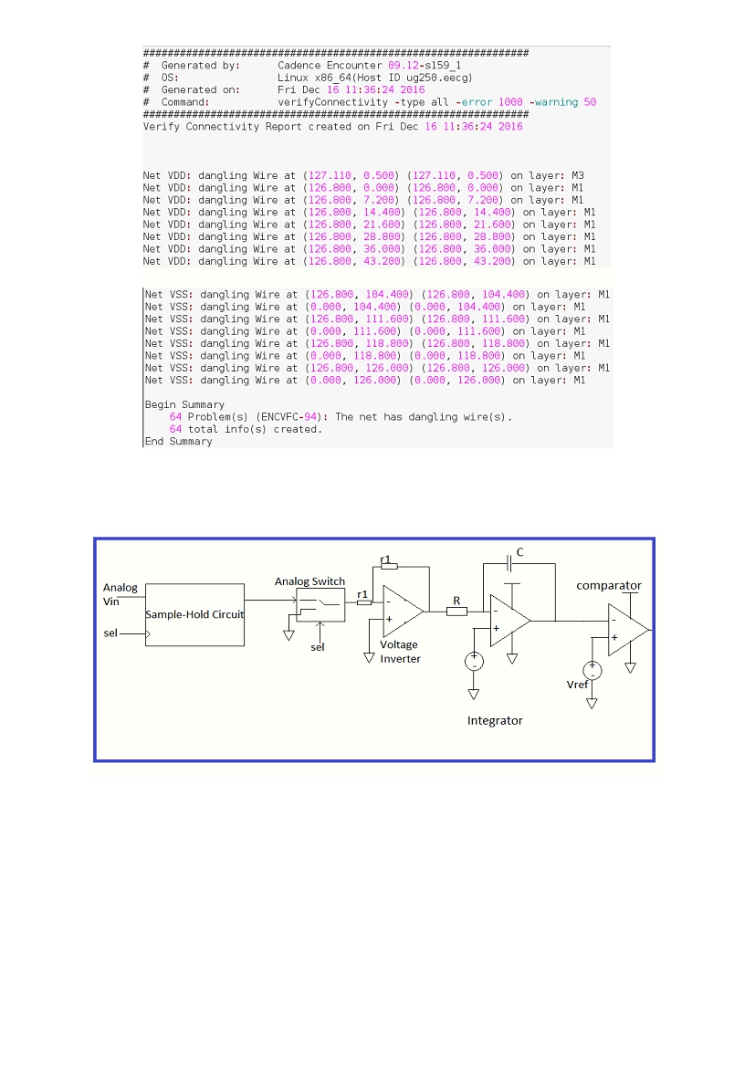
Figure 13.Parts of connectivity verification report, only returning ‘dangling VDD and VSS wires’, which is fixed when incorporated
with analog design
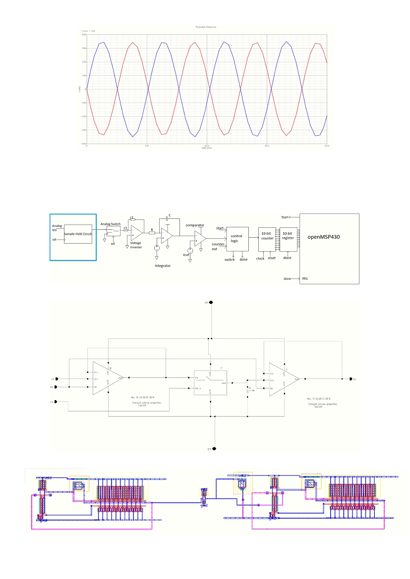
Analog Component of ADC (as highlighted in Blue in Figure 1):
Figure 14. Block Diagram highlighting the Analog Part of ADC
11
ECE1388 Final Project
openMSP430 Implementation-Dual Slope ADC
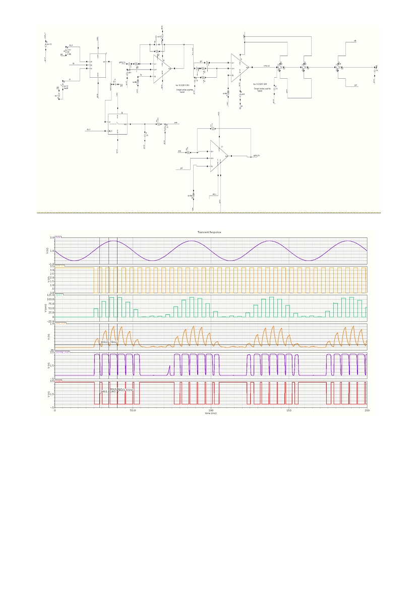
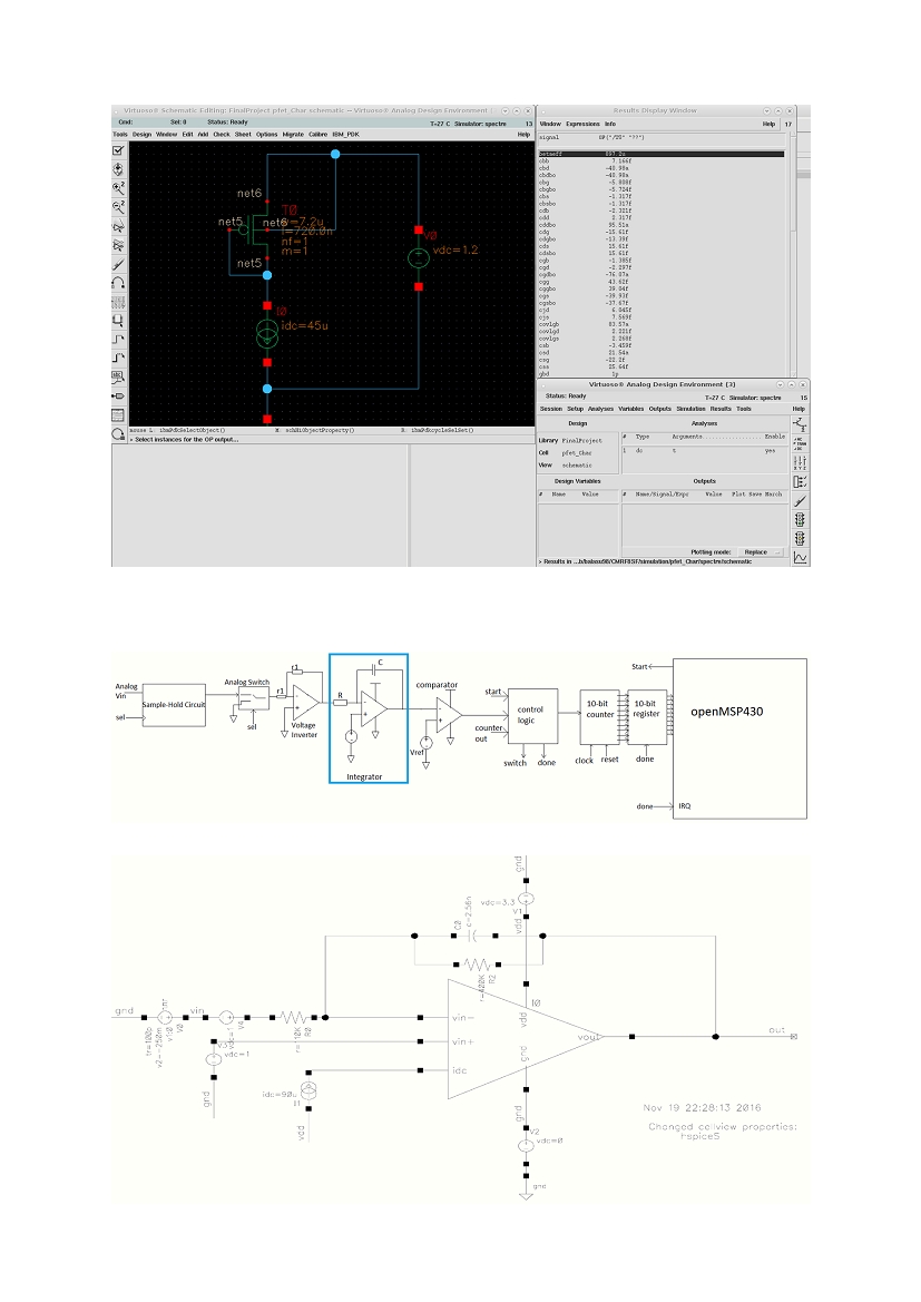
Figure 15. Top level schematic used for simulation of Analog design for the Dual Slope ADC
Figure 16. Waveforms obtained after simulating the above design
12
ECE1388 Final Project
openMSP430 Implementation-Dual Slope ADC
Op-Amp Design:
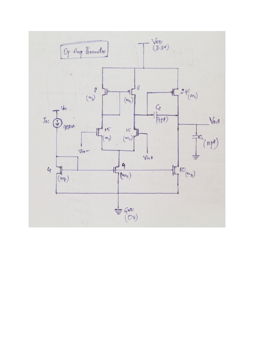
Figure 17. Circuit of op-amp designed (Hand Drawn) showing W/L ratios of individual transistors for the design constraints stated
13
ECE1388 Final Project
openMSP430 Implementation-Dual Slope ADC
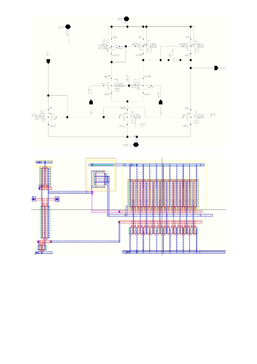
Figure 18. Schematic of op-amp designed in Analog Artist
Figure 19. Layout of Op-Amp
14
ECE1388 Final Project
openMSP430 Implementation-Dual Slope ADC
Supplementary (for op-amp design):
Characterization of NFET:
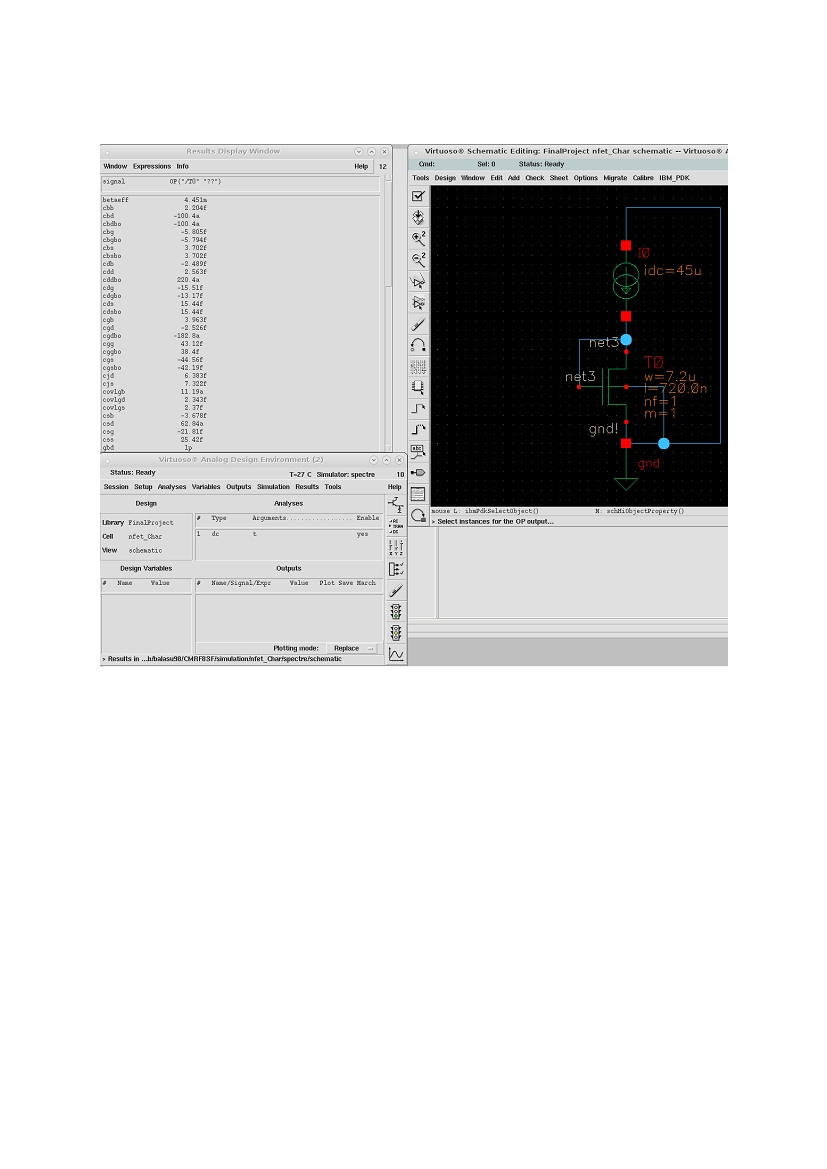
Figure 20. Schematic, Analog (DC analysis) environment, DC operating Point Conditions for the NMOS used in the design
15
ECE1388 Final Project
openMSP430 Implementation-Dual Slope ADC
Characterization of PFET:
Figure 21. Schematic, Analog (DC analysis) environment, DC operating Point Conditions for the PMOS used in the design
Op-Amp Integrator:
Figure 22. Block diagram highlighting the integrator
Figure 23. Schematic of Integrator designed in Analog Artist
16
ECE1388 Final Project
openMSP430 Implementation-Dual Slope ADC
Figure 24. Layout of Integrator
Figure 25. Simulation of Integrator
Op-Amp Comparator:
Figure 26. Block diagram highlighting the comparator
17
ECE1388 Final Project
openMSP430 Implementation-Dual Slope ADC
Figure 27. Schematic of the comparator designed in Analog Artist
Figure 28. Layout of Comparator
Figure 29. Simulation of Comparator
18
ECE1388 Final Project
openMSP430 Implementation-Dual Slope ADC
Op-Amp Analog Inverter:
Figure 30. Block diagram showing Analog Voltage Inverter
Figure 31. Schematic of Analog Inverter designed in Analog Artist
Figure 32. Layout of Analog Inverter
19
ECE1388 Final Project
openMSP430 Implementation-Dual Slope ADC
Figure 33. Simulation of Analog Inverter
Op-Amp based Sample-Hold:
Figure 34. Block diagram highlighting Sample-Hold circuit
Figure 35. Schematic (derived from symbols) of Sample-Hold circuit (designed in Analog Artist)
Figure 36. Layout of Sample-Hold circuit
20
ECE1388 Final Project
openMSP430 Implementation-Dual Slope ADC
Figure 37. Simulation of Sample Hold circuit
Transmission Gate based Analog Switch:
Figure 38. Block diagram showing Analog Switch
21
ECE1388 Final Project
openMSP430 Implementation-Dual Slope ADC
Figure 39. Schematic (symbol created) of Analog Switch (designed in Analog Artist)
Figure 40. Layout of Analog Switch
Figure 41. Simulation of Analog Switch
22
ECE1388 Final Project
openMSP430 Implementation-Dual Slope ADC
Top-Level Verification:
Figure 42. Top level schematic of the Analog design used for verification of the Dual Slope ADC, designed in Analog Artist using IBM 0.13 CMRF8SF Technology
Figure 43. Top-level layout of the Analog design of the Dual Slope ADC, designed in Cadence Virtuoso using IBM 0.13 CMRF8SF Technology
23
ECE1388 Final Project
openMSP430 Implementation-Dual Slope ADC
Figure 44. LVS for the top-level Analog design of ADC successfully passes
24

ECE1388 Final Project
openMSP430 Implementation-Dual Slope ADC
Top Level LVS Report (Analog component of ADC) :
##################################################
##
##
##
C A L I B R E S Y S T E M
##
##
##
##
L V S
R E P O R T
##
##
##
##################################################
REPORT FILE NAME:
final_full_toplevel.lvs.report
LAYOUT NAME:
final_full_toplevel.calibre.db
SOURCE NAME:
/nfs/ug/homes-4/w/wangj414/CMRF8SF/final_full_toplevel.netlist.lvs
('final_full_toplevel')
RULE FILE:
/nfs/ug/homes-4/w/wangj414/CMRF8SF/_cmrf8sf.lvs.cal_
LVS MODE:
Mask
RULE FILE NAME:
/nfs/ug/homes-4/w/wangj414/CMRF8SF/_cmrf8sf.lvs.cal_
CREATION TIME:
Fri Dec 16 17:31:37 2016
CURRENT DIRECTORY:
/nfs/ug/homes-4/w/wangj414/CMRF8SF
USER NAME:
wangj414
CALIBRE VERSION:
v2010.4_17.11
Thu Nov 18 13:38:14 PST 2010
*************************************************************************************************************
*
OVERALL COMPARISON RESULTS
*************************************************************************************************************
*
#
###################
_
_
#
#
#
*
*
#
#
#
CORRECT
#
|
# #
#
#
\___/
#
###################
-------------------------------------------------------------------------------------------------------------
-
INITIAL NUMBERS OF OBJECTS
--------------------------
Layout Source
Component Type
------ ------
--------------
Ports:
9
9
Nets:
2585
40
*
Instances:
126
31
*
MN (4 pins)
116
21
* MP (4 pins)
90
5
* R (3 pins)
16
0
* D (2 pins)
7
7
ncap (4 pins)
------ ------
Total Inst:
355
64
NUMBERS OF OBJECTS AFTER TRANSFORMATION
---------------------------------------
Layout Source
Component Type
------ ------
--------------
25

ECE1388 Final Project
openMSP430 Implementation-Dual Slope ADC
Ports:
9
9
Nets:
40
40
Instances:
28
28
MN (4 pins)
18
18
MP (4 pins)
5
5
R (3 pins)
7
7
ncap (4 pins)
3
3
INV (2 pins)
------ ------
Total Inst:
61
61
* = Number of objects in layout different from number in source.
*************************************************************************************************************
*
LVS PARAMETERS
*************************************************************************************************************
*
o LVS Setup:
LVS COMPONENT TYPE PROPERTY
element
LVS COMPONENT SUBTYPE PROPERTY
model
LVS PIN NAME PROPERTY
phy_pin
LVS POWER NAME
"VDD" "Vdd" "vdd" "VDD:P" "DVDD" "DVDD:P" "VDD!" "?VDD?" "vdd?"
"VCC" "Vcc" "vcc" "?VCC?"
"vcc?" "vddd" "vdd_33!" "vdda_33!" "VDDI" "VDDO" "PI"
LVS GROUND NAME
"VSS" "Vss" "vss" "VSS:G" "DVSS" "DVSS:P" "?VSS?" "vss?" "GND"
"GND:G" "GND!" "?GND?"
"sub!" "sub?" "sub_vss_33!" "sub_vssd_33!" "sub_vssa_33!" "VSSI"
"VSSO"
LVS CELL SUPPLY
NO
LVS RECOGNIZE GATES
ALL
LVS IGNORE PORTS
NO
LVS CHECK PORT NAMES
YES
LVS IGNORE TRIVIAL NAMED PORTS
NO
LVS BUILTIN DEVICE PIN SWAP
NO
LVS ALL CAPACITOR PINS SWAPPABLE
NO
LVS DISCARD PINS BY DEVICE
NO
LVS SOFT SUBSTRATE PINS
YES
LVS INJECT LOGIC
YES
LVS EXPAND UNBALANCED CELLS
YES
LVS FLATTEN INSIDE CELL
NO
LVS EXPAND SEED PROMOTIONS
NO
LVS PRESERVE PARAMETERIZED CELLS
NO
LVS GLOBALS ARE PORTS
YES
LVS REVERSE WL
NO
LVS SPICE PREFER PINS
NO
LVS SPICE SLASH IS SPACE
YES
LVS SPICE ALLOW FLOATING PINS
YES
// LVS SPICE ALLOW INLINE PARAMETERS
LVS SPICE ALLOW UNQUOTED STRINGS
NO
LVS SPICE CONDITIONAL LDD
NO
LVS SPICE CULL PRIMITIVE SUBCIRCUITS
NO
LVS SPICE IMPLIED MOS AREA
NO
// LVS SPICE MULTIPLIER NAME
LVS SPICE OVERRIDE GLOBALS
NO
LVS SPICE REDEFINE PARAM
NO
LVS SPICE REPLICATE DEVICES
YES
LVS SPICE SCALE X PARAMETERS
NO
LVS SPICE STRICT WL
NO
26

ECE1388 Final Project
openMSP430 Implementation-Dual Slope ADC
// LVS SPICE OPTION
LVS STRICT SUBTYPES
NO
LVS EXACT SUBTYPES
NO
LAYOUT CASE
YES
SOURCE CASE
YES
LVS COMPARE CASE
NO
LVS DOWNCASE DEVICE
NO
LVS REPORT MAXIMUM
50
LVS PROPERTY RESOLUTION MAXIMUM
ALL
// LVS SIGNATURE MAXIMUM
// LVS FILTER UNUSED OPTION
// LVS REPORT OPTION
LVS REPORT UNITS
YES
// LVS NON USER NAME PORT
// LVS NON USER NAME NET
// LVS NON USER NAME INSTANCE
// Reduction
LVS REDUCE SERIES MOS
NO
LVS REDUCE PARALLEL MOS
YES
LVS REDUCE SEMI SERIES MOS
NO
LVS REDUCE SPLIT GATES
NO
LVS REDUCE PARALLEL BIPOLAR
YES
LVS REDUCE SERIES CAPACITORS
NO
LVS REDUCE PARALLEL CAPACITORS
YES
LVS REDUCE SERIES RESISTORS
YES
LVS REDUCE PARALLEL RESISTORS
YES
LVS REDUCE PARALLEL DIODES
YES
LVS REDUCE R(opndres) SERIES POS NEG [ TOLERANCE w 0 l 0 ]
LVS REDUCE R(nwres) SERIES POS NEG [ TOLERANCE w 0 l 0 ]
LVS REDUCE R(opppcres)
SERIES POS NEG [ TOLERANCE w 0 l 0 bp 0 ]
LVS REDUCE R(oprrpres)
SERIES POS NEG [ TOLERANCE w 0 l 0 bp 0 ]
LVS REDUCE R(oprppres)
SERIES POS NEG [ TOLERANCE w 0 l 0 bp 0 ]
LVS REDUCE R(silres) SERIES POS NEG [ TOLERANCE w 0 l 0 bp 0 ]
LVS REDUCE R(l1res) SERIES POS NEG [ TOLERANCE w 0 l 0 ]
LVS REDUCE R(kxres) SERIES POS NEG [ TOLERANCE w 0 l 0 ]
LVS REDUCE R(lvsres) SERIES POS NEG
LVS REDUCE efuse SERIES IN OUT
LVS REDUCE MN(nfet) PARALLEL [ TOLERANCE L 0.5 psp 0 ]
LVS REDUCE MN(nfet33) PARALLEL [ TOLERANCE L 0.5 ]
LVS REDUCE M(lpnfet) PARALLEL [ TOLERANCE L 0.5 ]
LVS REDUCE M(zvtnfet) PARALLEL [ TOLERANCE L 0.5 ]
LVS REDUCE M(hvtnfet33)
PARALLEL [ TOLERANCE L 0.5 psp 0 ]
LVS REDUCE M(hvtnfet33_rf)
PARALLEL [ TOLERANCE ring 0 L 0.5 psp 0 ]
LVS REDUCE M(hvtpfet33)
PARALLEL [ TOLERANCE L 0.5 psp 0 ]
LVS REDUCE M(hvtpfet33_rf)
PARALLEL [ TOLERANCE ring 0 L 0.5 psp 0 ]
LVS REDUCE MD(dgnfet) PARALLEL [ TOLERANCE L 0.5 psp 0 ]
LVS REDUCE M(zvtdgnfet)
PARALLEL [ TOLERANCE L 0.5 ]
LVS REDUCE M(lvtnfet) PARALLEL [ TOLERANCE L 0.5 ]
LVS REDUCE MN(nfet_rf)
PARALLEL [ TOLERANCE ring 0 L 0.5 psp 0 ]
LVS REDUCE MN(nfet33_rf)
PARALLEL [ TOLERANCE ring 0 L 0.5 ]
LVS REDUCE M(lpnfet_rf)
PARALLEL [ TOLERANCE ring 0 L 0.5 ]
LVS REDUCE MD(dgnfet_rf)
PARALLEL [ TOLERANCE ring 0 L 0.5 psp 0 ]
LVS REDUCE M(lvtnfet_rf)
PARALLEL [ TOLERANCE ring 0 L 0.5 ]
LVS REDUCE MP(pfet) PARALLEL [ TOLERANCE L 0.5 psp 0 ]
LVS REDUCE MP(pfet33) PARALLEL [ TOLERANCE L 0.5 ]
LVS REDUCE M(lppfet) PARALLEL [ TOLERANCE L 0.5 ]
LVS REDUCE MD(dgpfet) PARALLEL [ TOLERANCE L 0.5 psp 0 ]
LVS REDUCE M(lvtpfet) PARALLEL [ TOLERANCE L 0.5 ]
LVS REDUCE MP(pfet_rf)
PARALLEL [ TOLERANCE ring 0 L 0.5 psp 0 ]
LVS REDUCE MP(pfet33_rf)
PARALLEL [ TOLERANCE ring 0 L 0.5 ]
LVS REDUCE M(lppfet_rf)
PARALLEL [ TOLERANCE ring 0 L 0.5 ]
LVS REDUCE MD(dgpfet_rf)
PARALLEL [ TOLERANCE ring 0 L 0.5 psp 0 ]
LVS REDUCE M(lvtpfet_rf)
PARALLEL [ TOLERANCE ring 0 L 0.5 ]
27

ECE1388 Final Project
openMSP430 Implementation-Dual Slope ADC
LVS REDUCE R(opndres) PARALLEL [ TOLERANCE l 0 w 0 ]
LVS REDUCE R(nwres) PARALLEL [ TOLERANCE l 0 w 0 ]
LVS REDUCE R(opppcres)
PARALLEL [ TOLERANCE l 0 w 0 bp 0 ]
LVS REDUCE R(oprrpres)
PARALLEL [ TOLERANCE l 0 w 0 bp 0 ]
LVS REDUCE R(oprppres)
PARALLEL [ TOLERANCE l 0 w 0 bp 0 ]
LVS REDUCE R(silres) PARALLEL [ TOLERANCE l 0 w 0 bp 0 ]
LVS REDUCE R(l1res) PARALLEL [ TOLERANCE l 0 w 0 ]
LVS REDUCE R(kxres) PARALLEL [ TOLERANCE l 0 w 0 ]
LVS REDUCE R(lvsres) PARALLEL
LVS REDUCE ncap PARALLEL [ TOLERANCE w 0 l 0 ]
LVS REDUCE dgncap PARALLEL [ TOLERANCE w 0 l 0 ]
LVS REDUCE C(vncap) PARALLEL [ TOLERANCE bp 0 w 0 l 0 ]
LVS REDUCE D(havar) PARALLEL [ TOLERANCE w 0 l 0 ]
LVS REDUCE diffhavar PARALLEL [ TOLERANCE w 0 l 0 ]
LVS REDUCE diffncap PARALLEL [ TOLERANCE w 0 l 0 mSwitch 0 ]
LVS REDUCE D(sbd) PARALLEL [ TOLERANCE w 0 l 0 nf 0 ]
LVS REDUCE D(dipdnw) PARALLEL [ TOLERANCE w 0 l 0 nf 0 ]
LVS REDUCE Q(divpnp) PARALLEL
LVS REDUCE Q(esdvpnp) PARALLEL [ TOLERANCE nf 0 areae 0 areab 0 ]
LVS REDUCE D(esdndsx) PARALLEL [ TOLERANCE bp 0 ]
LVS REDUCE D(tdpdnw) PARALLEL
LVS REDUCE D(tdndsx) PARALLEL
LVS REDUCE subc PARALLEL
LVS REDUCE efuse PARALLEL
LVS REDUCTION PRIORITY
PARALLEL
// Filter
LVS FILTER D(diodenx) OPEN
LVS FILTER D(diodenwx)
OPEN
LVS FILTER D(diodepisx)
OPEN
LVS FILTER D(diodendsx)
OPEN
LVS FILTER D(diodepwpi)
OPEN
LVS FILTER D(diodepnw)
OPEN
*************************************************************************************************************
*
INFORMATION AND WARNINGS
*************************************************************************************************************
*
Matched Matched
Unmatched
Unmatched
Component
Layout Source
Layout
Source
Type
------- -------
---------
---------
---------
Ports:
9
9
0
0
Nets:
40
40
0
0
Instances:
28
28
0
0
MN(nfet)
18
18
0
0
MP(pfet)
5
5
0
0
R(silres)
7
7
0
0
ncap
3
3
0
0
INV
------- -------
---------
---------
Total Inst:
61
61
0
0
o Statistics:
2460 isolated layout nets were deleted.
16 layout instances were filtered and their pins removed from adjoining nets.
28

ECE1388 Final Project
openMSP430 Implementation-Dual Slope ADC
200 layout mos transistors were reduced to 10.
190 mos transistors were deleted by parallel reduction.
90 series layout resistors were reduced to 5.
85 connecting nets were deleted.
o Isolated Layout Nets:
(Layout nets which are not connected to any instances or ports).
126(54.530,109.310) 127(65.060,139.690) 128(65.860,139.690) 129(86.260,136.030)
130(87.060,136.030) 131(87.860,136.030) 132(88.660,136.030) 133(89.460,136.030)
134(90.260,136.030) 135(91.060,136.030) 136(91.860,136.030) 137(92.660,136.030)
138(93.460,136.030) 139(94.260,136.030) 140(95.060,136.030) 141(95.860,136.030)
142(96.660,136.030) 143(97.460,136.030) 144(98.260,136.030) 145(99.060,136.030)
146(99.860,136.030) 147(100.660,136.030) 148(101.460,136.030) 149(114.090,137.440)
150(139.450,140.450) 151(140.250,140.450) 152(160.650,136.790) 153(161.450,136.790)
154(162.250,136.790) 155(163.050,136.790) 156(163.850,136.790) 157(164.650,136.790)
158(165.450,136.790) 159(166.250,136.790) 160(167.050,136.790) 161(167.850,136.790)
162(168.650,136.790) 163(169.450,136.790) 164(170.250,136.790) 165(171.050,136.790)
166(171.850,136.790) 167(172.650,136.790) 168(173.450,136.790) 169(174.250,136.790)
170(175.050,136.790) 171(175.850,136.790) 172(193.980,130.600) 173(193.980,141.290)
174(225.550,138.490) 175(226.350,138.490)
o Initial Correspondence Points:
Ports:
VDD GND clk_in clk_in_inv idc vout vin SW_ SW
*************************************************************************************************************
*
SUMMARY
*************************************************************************************************************
*
Total CPU Time:
1 sec
Total Elapsed Time: 2 sec
29
ECE1388 Final Project
openMSP430 Implementation-Dual Slope ADC
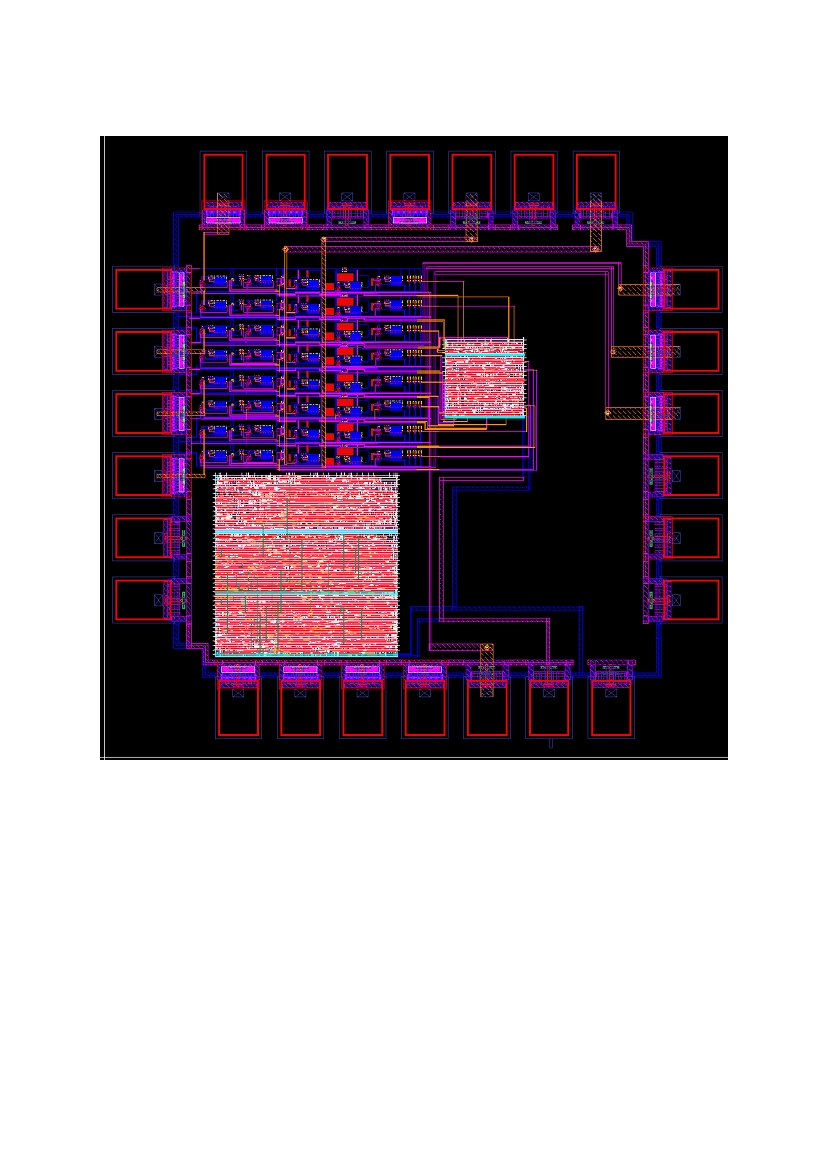
Pad Frame Layout:
Figure 45. Un-annotated pad frame layout containing openMSP430, analog and digital design of the ADC
30
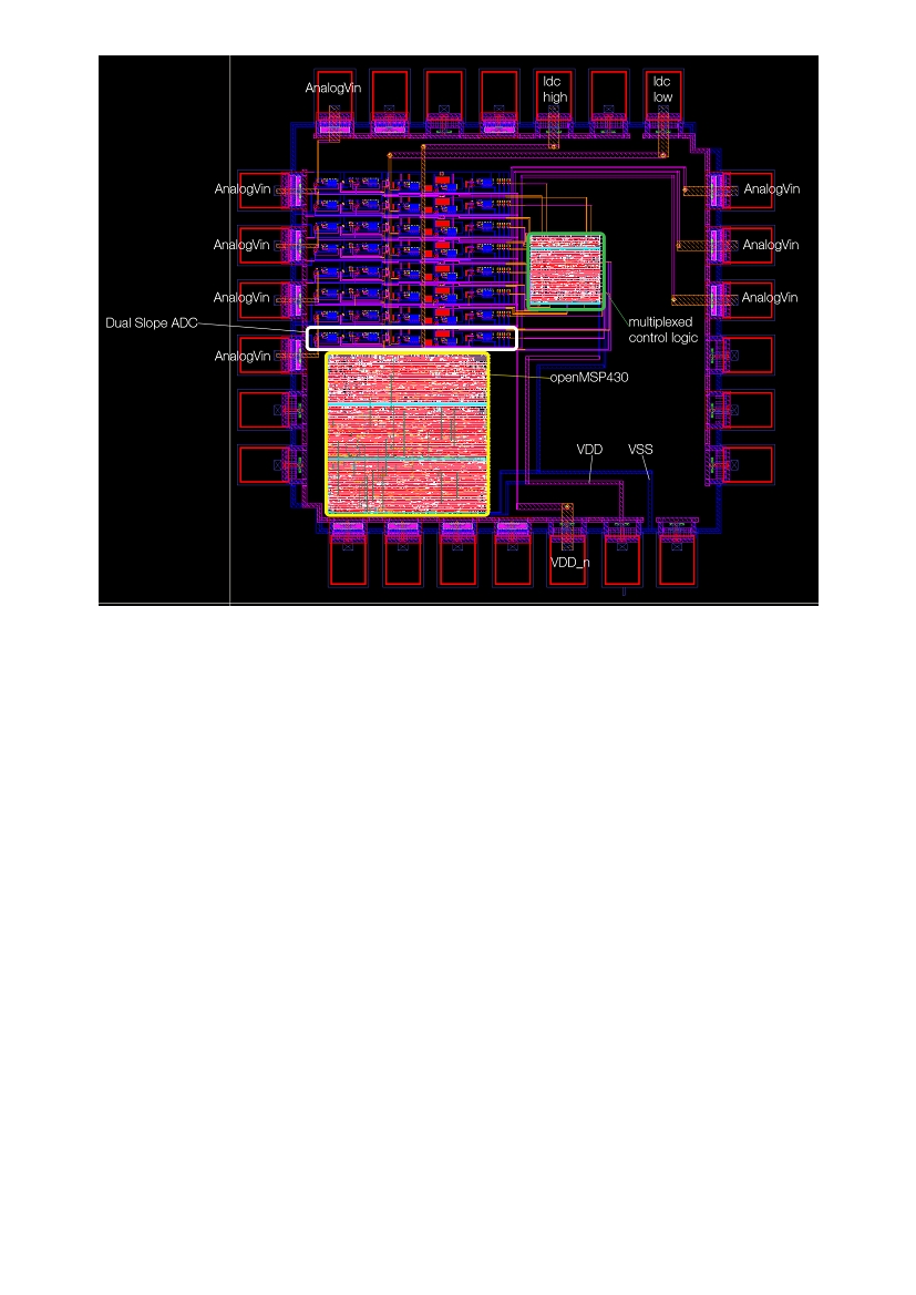
ECE1388 Final Project
openMSP430 Implementation-Dual Slope ADC
Figure 46. Annotated pad frame
31
ECE1388 Final Project
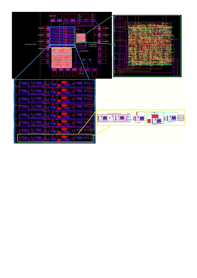
openMSP430 Implementation-Dual Slope ADC
Figure 47. Blown-up components from pad frame
32
ECE1388 Final Project
openMSP430 Implementation-Dual Slope ADC
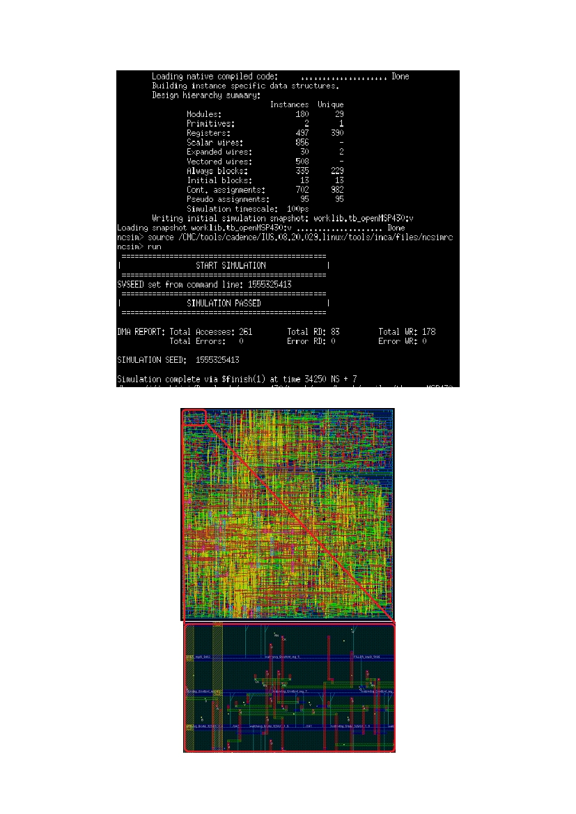
openMSP430:
Figure 48. Example simulation of a module of the openMSP430 core
Figure 49. OpenMSP430 Placed and routed design with blown up image of ‘Watch Dog’ section as example
33
ECE1388 Final Project
openMSP430 Implementation-Dual Slope ADC
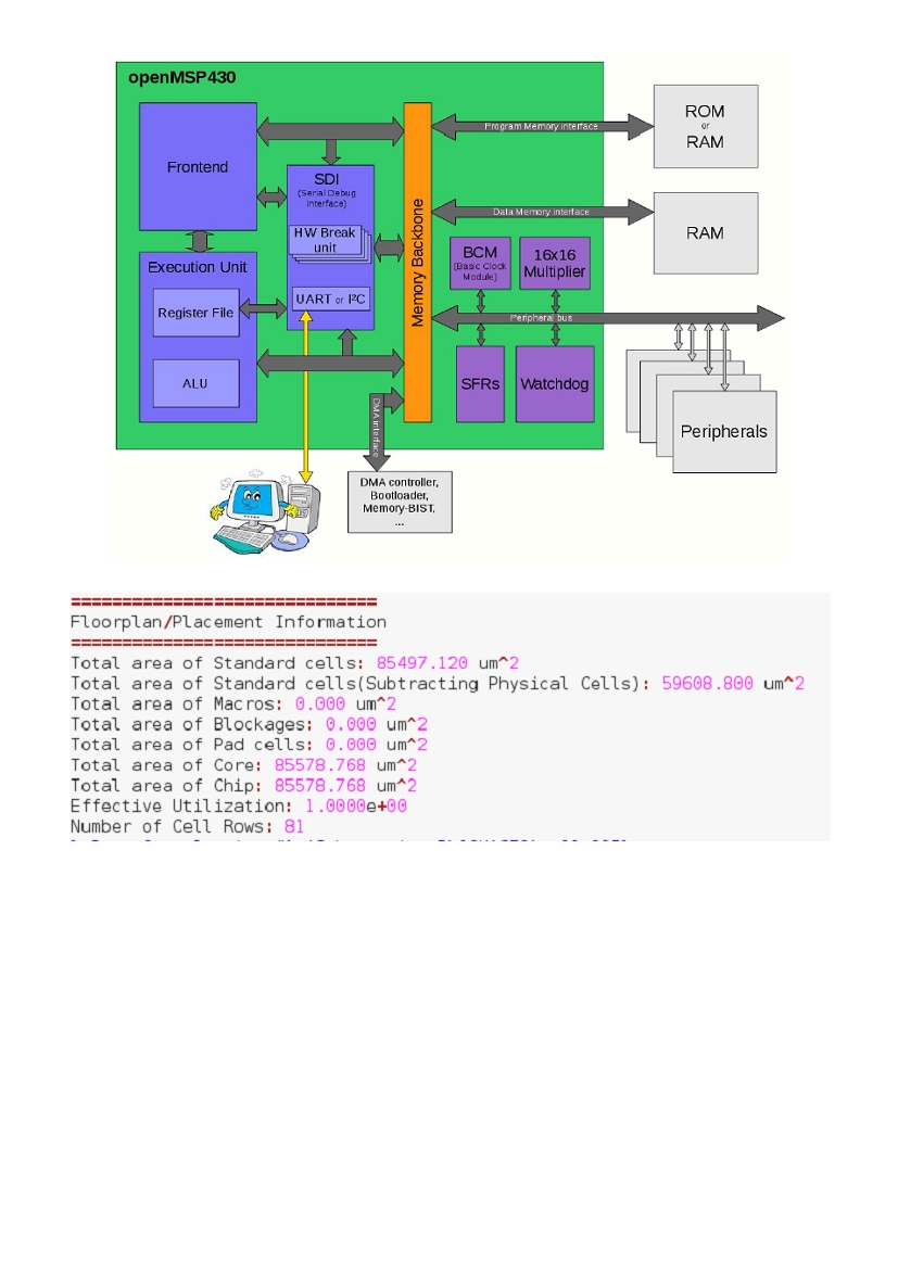
Figure 50 . openMSP430 Block Diagram. Source – openMSP430 documentation[4]
Figure 51. Area report of openMSP430 generated by Cadence Encounter
34
ECE1388 Final Project
openMSP430 Implementation-Dual Slope ADC
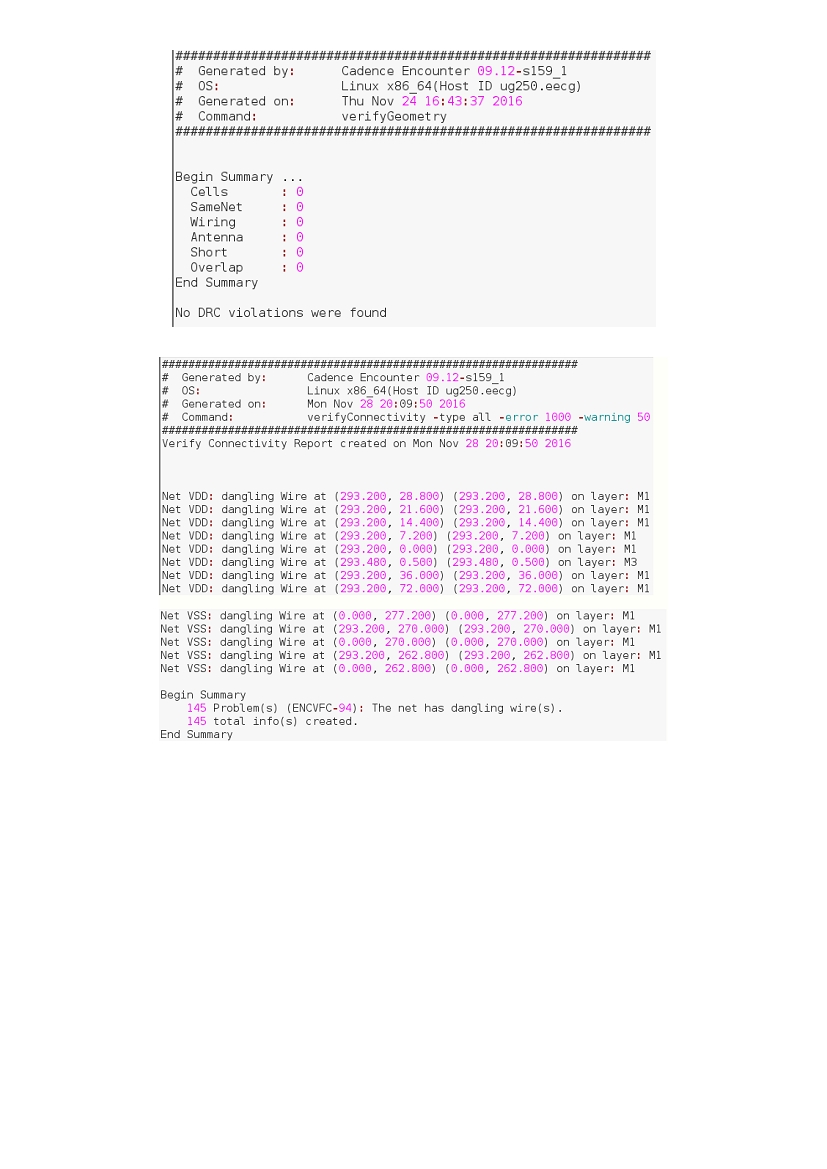
Figure 52. No DRC errors returned in openMSP430 geometry verification report
Figure 53. Parts of connectivity verification report, only returning ‘dangling VDD and VSS wires’, which is fixed when incorporated
with analog design
35

ECE1388 Final Project
openMSP430 Implementation-Dual Slope ADC
References
[1]Atmel http://www.atmel.com/devices/atmega328p.aspx?tab=parameters
[2]Atmel - http://www.atmel.com/Images/Atmel-42735-8-bit-AVR-Microcontroller-ATmega328-
328P_datasheet.pdf
[3]Circuits Today- http://www.circuitstoday.com/introduction-to-pic-16f877
[4]Girard, O -
http://opencores.org/websvn,filedetails?repname=openmsp430&path=%2Fopenmsp430%2Ftrunk%
2Fdoc%2FopenMSP430.pdf
[5]Maxim Integrated - pdfserv.maximintegrated.com/en/an/AN2094.pdf
[6]Microchip http://www.microchip.com/wwwproducts/en/PIC16F877A
[7]Presser, M - http://iot.ieee.org/newsletter/january-2016/the-rise-of-iot-why-today.html
[8]Texas Instruments - http://www.ti.com/lit/ds/symlink/msp430g2453.pdf
36

ECE1388 Final Project
openMSP430 Implementation-Dual Slope ADC
End of Report
37