ECE 1388 Final Project
Sensor Signal Processing Block
Genwen Zhao, Yifeng
Zhang, Weigen Yuan, Qijun Wen
1
Overview
Sensor
technology has increasing demands over various applications in different aspects
of our daily life and society. Low power design has also become one of the
biggest challenges in IC design. This report describes the implementation of a
Sensor Signal Processing Block, which consists of a 6-bit flash ADC and a 16-bit
general purpose microcontroller openMSP430, in IBM 0.13um CMOS technology with
low power technique to minimize the power consumption of the whole system.
2
System outline
The block
diagram of the Sensor Signal Processing Block is shown in Figure
1. Some external CMOS sensors will be
used to detect the changes of the outside world and send the corresponding
analog signals to our design. After receiving the analog signals, the 6-bit
flash ADC will convert the analog signal into a 6-bit digital signal and openMSP430
will be used to process the signals.
3
Block design
3.1 Digital openMSP430 Microcontroller
OpenMSP430 is a 16 bit general purpose microcontroller, featuring low power consumption with clock gating technique [1]. Its architecture Figure 2 contains the following sub-blocks:
Frontend Module -- Instruction decode and fetch, execution state decode
Execution Unit -- ALU that executes the decoded instructions according to execution state
Serial Debug Interface -- Standard two-wire debug interface
Memory Backbone -- Data transfer management between memory and functional blocks
Basic Clock Module -- Generates MCLK, ACLK and SMCLK, manages low power modes
OpenMSP430 has been implemented with IBM 0.13um technology using standard digital implementation methodology. Its functionality has been verified by running gate level simulation and confirmed timing clean on post-route netlist. DRC check passed with some acceptable waivers. However, due to the tool issues and time constraints, LVS hasn't been performed successfully in Cadence at this point. Figure 3-9 show all implementation results.
3.2 6-bit Flash ADC
3.2.1 Specifications of 6 bit Flash ADC
The maximum sampling rate of the ADC is 22MHz with a full scale input of 0.235 – 0.97V at a common mode input of 0.6V. The power consumption is about 20.09mW at 1.2V VDD and 22MHz input clock frequency. A transient simulation is performed at 22MHz clock frequency to show the correct operation of the ADC. Details see Figure 10-13.
3.2.2 Resistor Ladder
A resistor ladder is used to distribute the reference voltages ranging from 0.242 – 0.961V with VLSB of 11.3mV to the comparators. Decoupling capacitors (500fF each) are added on each reference node to reduce the noise coming from the comparators. The resistor ladder consumes about 67.55uW of static power. The layout is incorporated into the analog frontend layout of the Flash ADC. Details see Figure 14-15.
3.2.3 Track and Hold
This circuit tracks the input voltage at clock running high and the op-amp buffers the voltage out to the comparator when the clock is low [2]. The maximum sampling rate is 350MHz which is the unity gain bandwidth of the op-amp. The power consumption is about 307.5uW at 22MHz clock without the biasing circuit. The circuit, layout and simulation are shown in Figure 16-21.
3.2.4 Comparator
The strongArm comparator consumes zero static power and only 4.752uW of dynamic power at 22MHz [3]. The settling time of the comparator (22.5ns) at its threshold (0.235V) limits the maximum sampling rate of the ADC to 22MHz. The circuit, layout and simulation are shown in Figure 22-24.
3.2.5 Registers (DFF)
Registers are used after comparator and before thermometer and encoder, because the later stages – thermometer and encoder – are both asynchronous; that is any fluctuation in the analog input to the comparator might be captured in the final binary output. In order to stabilize the output of comparator, we used a register implemented by the master-slave flip-flop. The schematic, layout and simulation of this cell are shown in Figure 25-27.
3.2.6 Thermometer
The thermometer is used to transform unary code (output from comparators) into one-hot code. Another function of this thermometer is to remove single bubble errors, increasing the stability of the system [2]. In our design, the thermometer (slice) is comprised of three NAND gates and one inverter. The schematic, layout (slice) and simulation of this cell are shown in Figure 28-30.
3.2.7 Encoder
For each output bit of an encoder, 32 OR gates are utilized. Much effort was put into fitting the layout of an encoder slice into a rectangular shape. The schematic, layout and simulation of this cell are shown in shown in Figure 31-33.
4
Layout and Pad Frame
The complete layout including pads is shown in Figure 37. The total area of the design is 4mm^2(2mm by 2mm). The pad frame was designed using the PAD_P13 library, which includes 4 different pad types, GND, power, signal with ESD protection and signal without ESD protection. The pad frame of our design has 75 pads, including 2 GND pads, 2 power pads, and 71 signal pads with ESD protection. See schematic and layout in Figure 34-35.
5
Conclusion
The team
was able to fully implement both analog ADC and digital openMSP430, and
integrate them into the top level. Analog ADC was able to achieve LVS (with
PAD) and DRC clean, see Figure 36-39.
Digital openMSP430 was able to achieve DRC clean, but LVS was not yet performed
at this point due to some setup issues.
6
Division of tasks
|
Task |
Genwen
Zhao |
Yifeng
Zhang |
Weigen
Yuan |
Qijun
Wen |
|
System Specification and Design |
X |
X |
X |
X |
|
|
|
|
|
|
|
OpenMSP430 Digital Implementation |
|
|
|
|
|
RTL
simulation |
X |
|
|
X |
|
Gate
level simulation |
X |
|
|
X |
|
RTL
Synthesis |
X |
|
|
|
|
Place and
Route |
X |
|
|
|
|
|
|
|
|
|
|
6 bit Flash ADC Implementation - Schematic, Layout and Simulation |
|
|
|
|
|
Resistor
Ladder |
|
X |
|
|
|
Track and
Hold |
|
X |
|
|
|
Comparator
|
|
X |
|
X |
|
Register
(DFF) |
|
X |
|
X |
|
Thermometer
|
|
|
X |
|
|
Encoder |
|
|
X |
|
|
|
|
|
|
|
|
System Integration |
|
|
|
|
|
Pad frame |
|
X |
X |
X |
|
Block/Top
level DRC and LVS |
X |
X |
X |
X |
7
Reference
[1] http://opencores.org/project,openmsp430
[2] Carusone, Tony Chan., Kenneth
William. Martin, and David Johns. Analog Integrated Circuit Design, 2nd
Edition. Hoboken, NJ: John Wiley & Sons, 2011. 675-77. Print.
[3] A. Abidi and H. Xu, "Understanding the regenerative
comparator circuit," Proceedings
of the IEEE 2014 Custom Integrated Circuits Conference, San Jose, CA,
2014, pp. 1-8.
8
Appendix
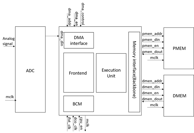
Figure 1: System Block Diagram
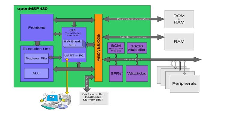
Figure 2: openMSP430 architecture [1]
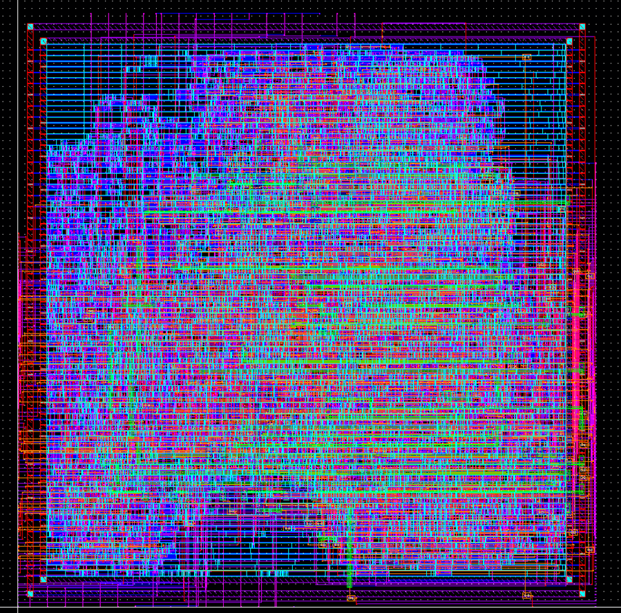
Figure 3: openMSP430 Layout
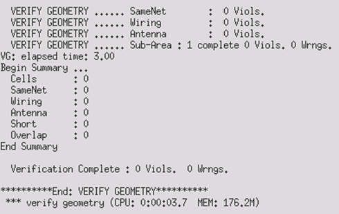
Figure 4:
Encounter Geometry Check
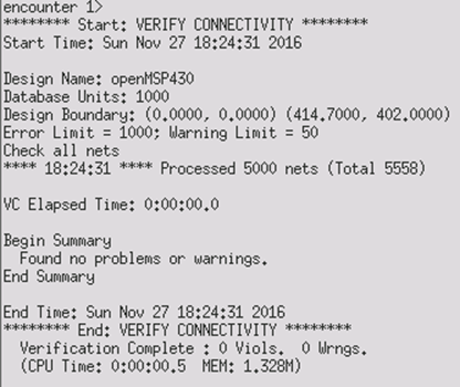
Figure 5 :
Encounter Connectivity Check
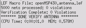
Figure 6:
Encounter Antenna Check
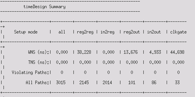
Figure 7:
Encounter Timing Result
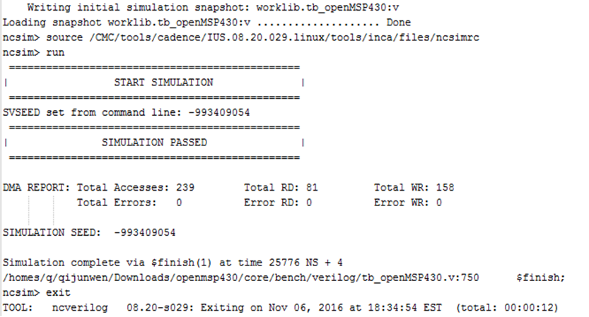
Figure 8: Gate
level Simulation Result
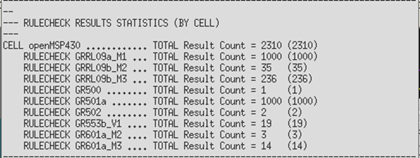
Figure 9:
openMSP430 DRC Result
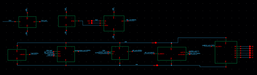
Figure 10: Flash_ADC Schematic
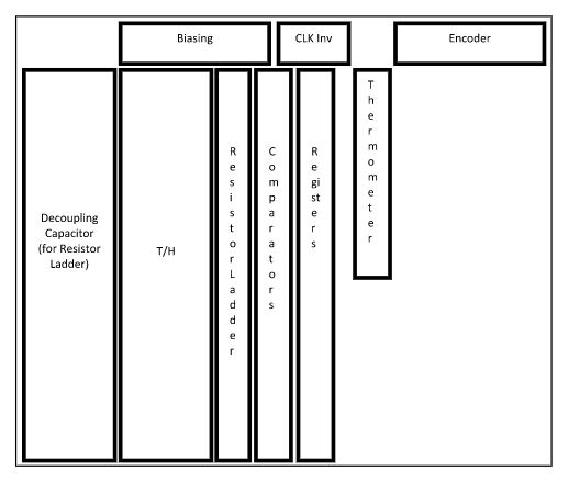
Figure 11: Flash_ADC Block Diagram
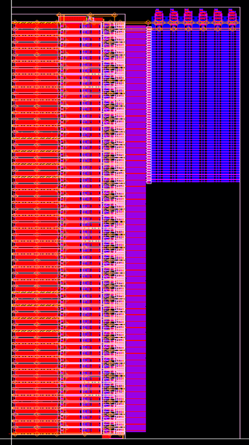
Figure 12: Flash_ADC Layout
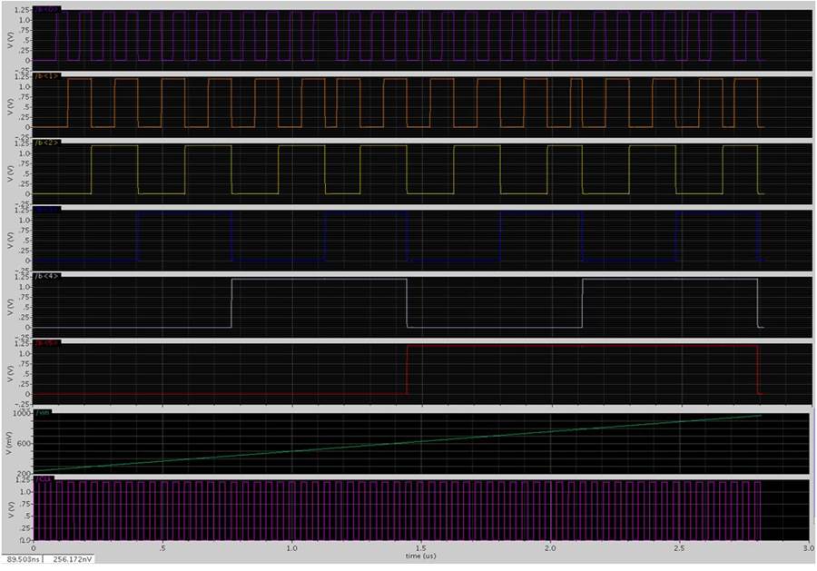
Figure 13: Flash_ADC Simulation
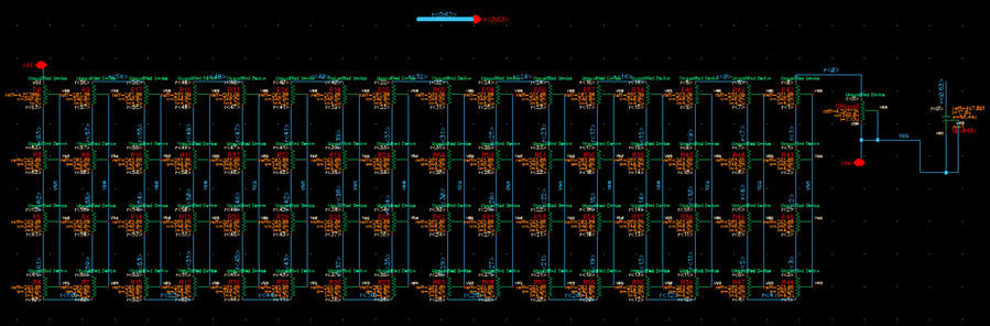
Figure 14: Resistor Ladder Schematic
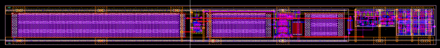
Figure 15: Analog FrontEnd Layout (repeated 64 times) with 1 Resistor, 1
Capacitor, SH, strongArm, DFF
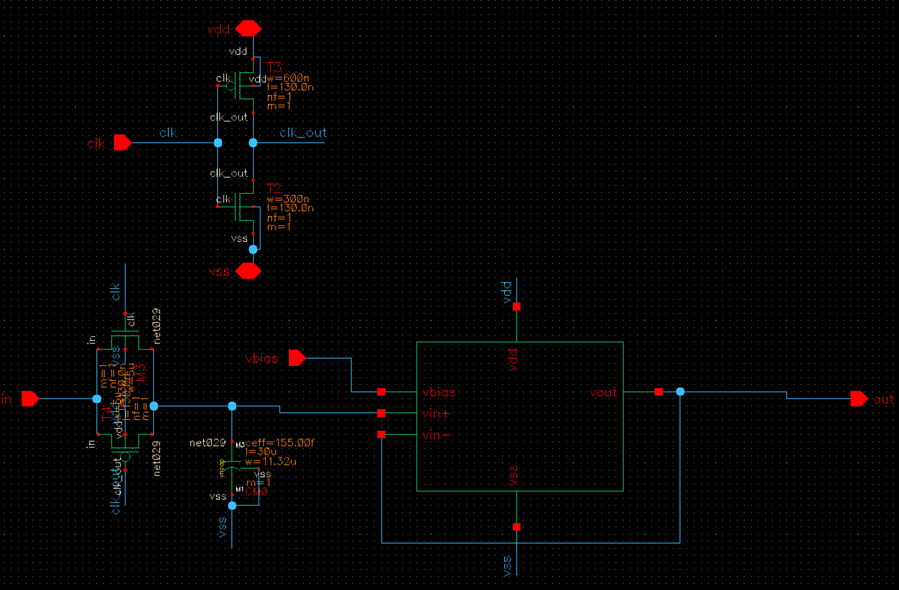
Figure 16: Track and Hold Schematic
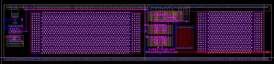
Figure 17: Track
and Hold Layout
Figure 18: Track
and Hold Simulation
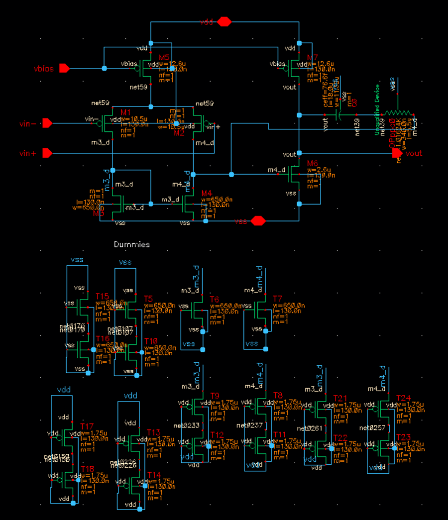
Figure 19: Op-amp Schematic
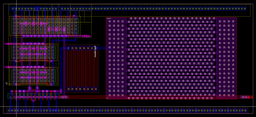
Figure 20: Op-amp
Layout
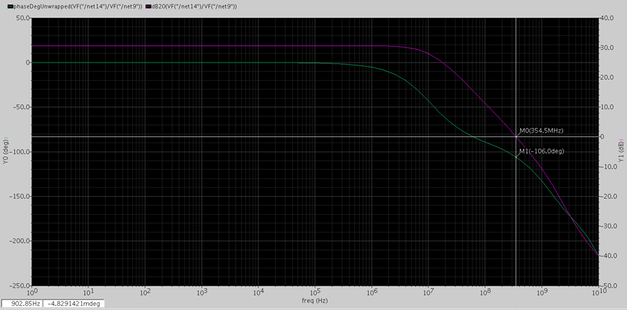
Figure 21: Op-amp
Simulation
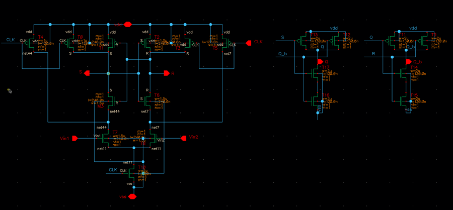
Figure 22: Comparator Schematics – strongArm
(left) and SR Latch (right)
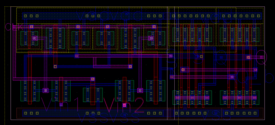
Figure 23:
Comparator Layout
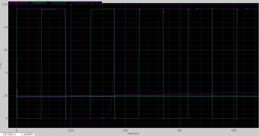
Figure 24:
Comparator Simulation
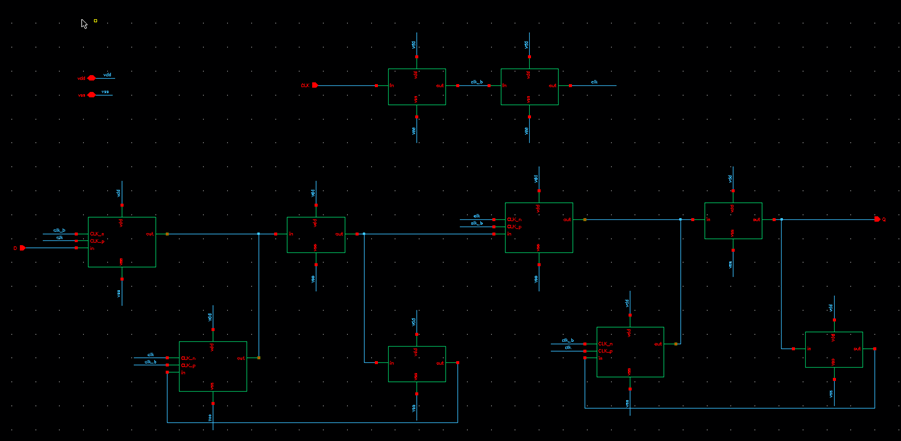
Figure 25: Register Schematic
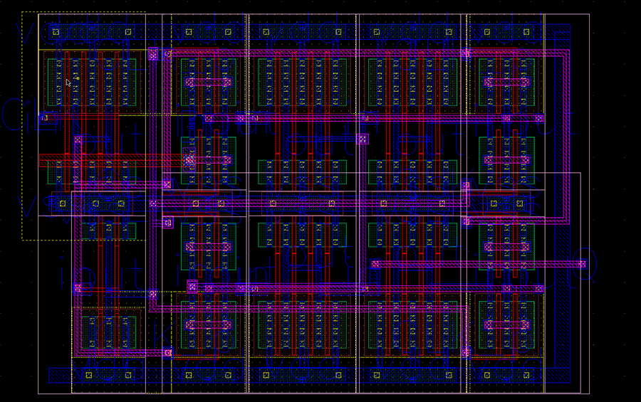
Figure 26:
Register Layout
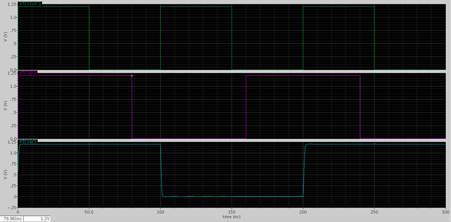
Figure 27:
Register Simulation
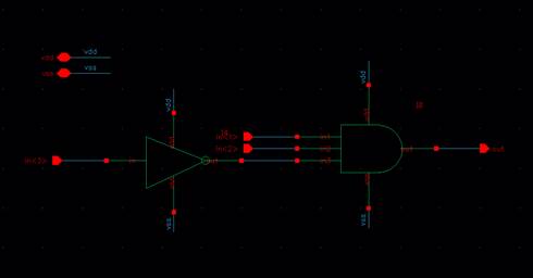
Figure 28: Thermometer Schematic
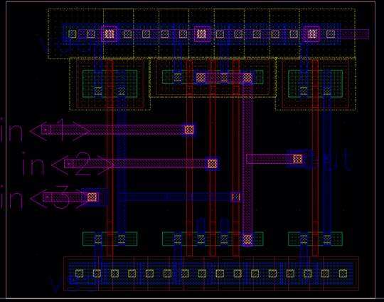
Figure 29:
Thermometer Layout
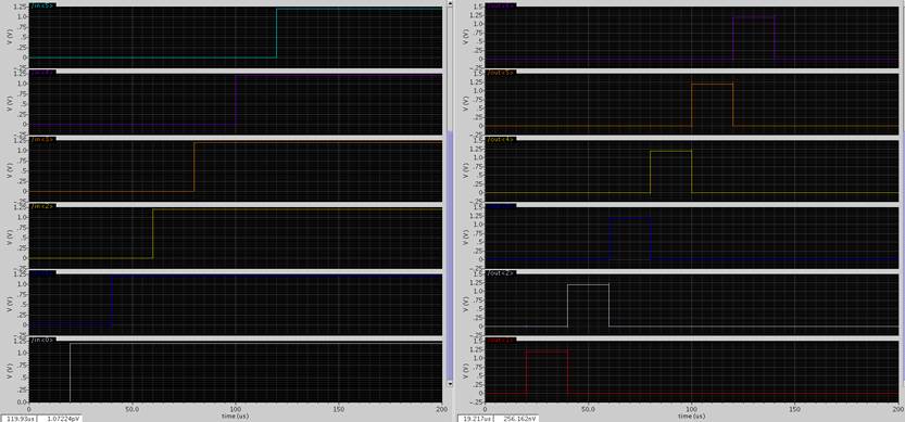
Figure 30:
Thermometer Simulation (input on the left, output on the right)
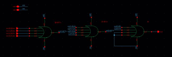
Figure 31: Encoder Schematic
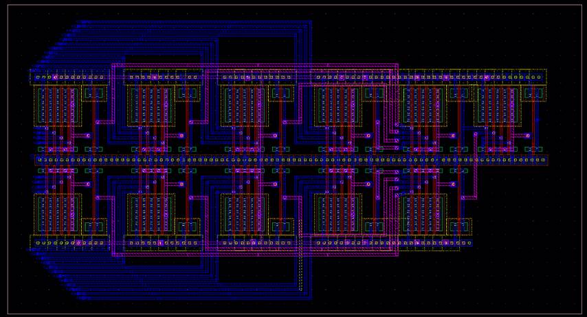
Figure 32: Encoder
Layout
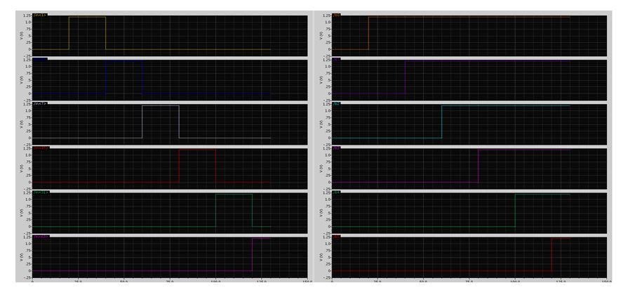
Figure 33: Encoder
Simulation
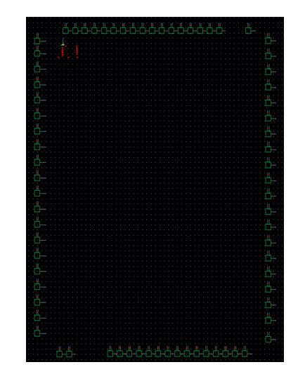
Figure 34: Pad Frame Schematic
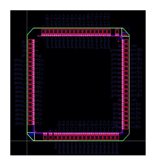
Figure 35: Pad
Frame Layout
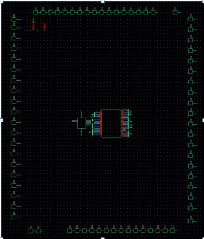
Figure 36: top level design schematic
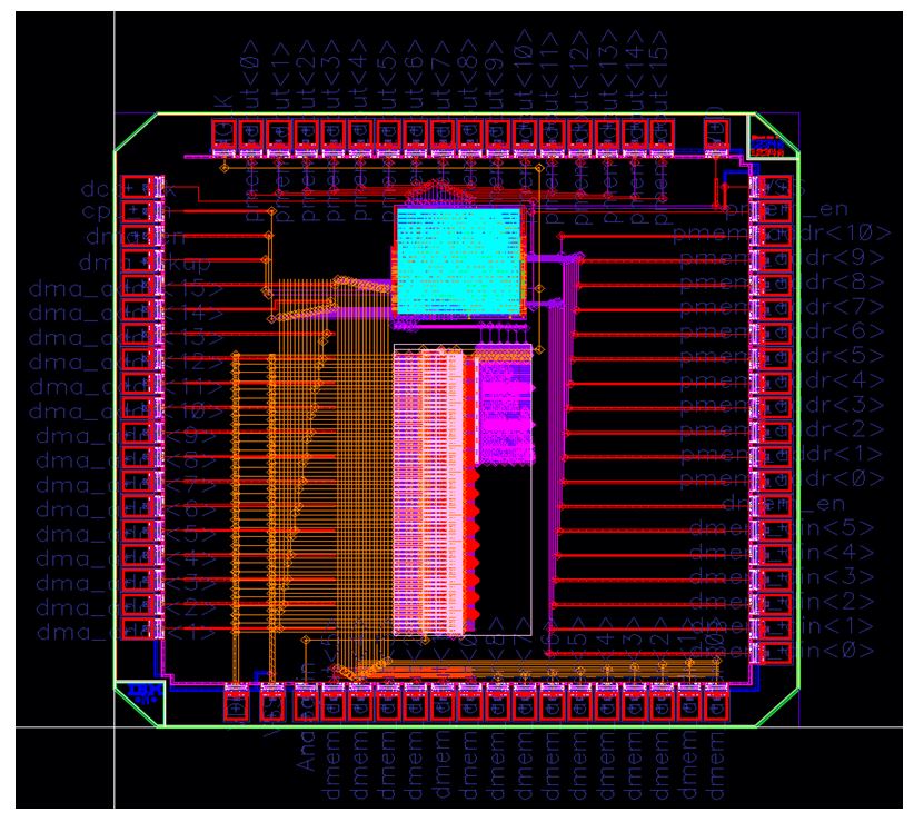
Figure 37: Top level design Layout
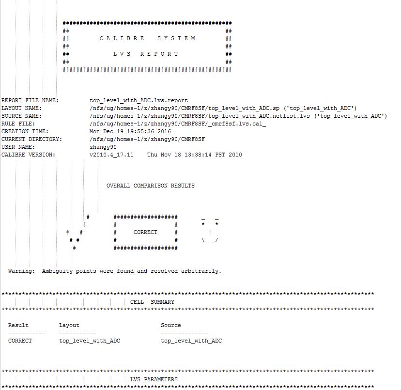
Figure 38: Top
level with ADC and PAD LVS result
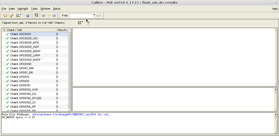
Figure 39: Flash
ADC DRC result