ZSTT: A Ferroelectric Capacitor Macromodel:
This page provides detailed description of a ferroelectric
capacitor macromodel, called Zero Switching Time Transient
(ZSTT) Model.
Zero Switching-Time Transient (ZSTT) Model:
As its name suggests, the ZSTT model assumes the switching time
of a ferroelectric capacitor to be zero.
This assumption will introduce little inaccuracy if the RC time
constant of the circuit under study is much
larger than the switching time of the FE capacitor. It is shown
[1] that for a typical memory circuit
including FE capacitors such an assumption is quite valid.
Zero switching-time implies that a charge increment on the FE
capacitor will take place
instantaneously. Therefore, a charge increment is only a function
of the applied voltage and the initial
state of the capacitor, not a function of time. In other words:
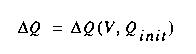 where V and Qinit represent the applied voltage and the initial
polarization charge on the capacitor. Since
there are only two initial states that are important to a memory
cell (i.e. digital 0 and 1), the above equation
can be broken into two parts, each corresponding to one initial
state. In other words:
where V and Qinit represent the applied voltage and the initial
polarization charge on the capacitor. Since
there are only two initial states that are important to a memory
cell (i.e. digital 0 and 1), the above equation
can be broken into two parts, each corresponding to one initial
state. In other words:
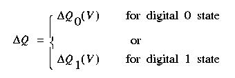 This equation is further represented as a state diagram:
 A positive voltage pulse, for example,
brings the capacitor to a digital 0 state if it is initially in a
digital 1 state. This state transition corresponds to
a charge increment of DQ1 followed by a charge decrement of
DQ0 -both of them functions of the pulse
amplitude. The pulse-measurement approach discussed in [1]
approximates DQ0(V) and DQ1(V) with two
piecewise-linear functions of voltage. Each piecewise-linear
function is implemented as a piecewise-linear
capacitor that exists in most circuit simulators.
A positive voltage pulse, for example,
brings the capacitor to a digital 0 state if it is initially in a
digital 1 state. This state transition corresponds to
a charge increment of DQ1 followed by a charge decrement of
DQ0 -both of them functions of the pulse
amplitude. The pulse-measurement approach discussed in [1]
approximates DQ0(V) and DQ1(V) with two
piecewise-linear functions of voltage. Each piecewise-linear
function is implemented as a piecewise-linear
capacitor that exists in most circuit simulators.
model Implementation:
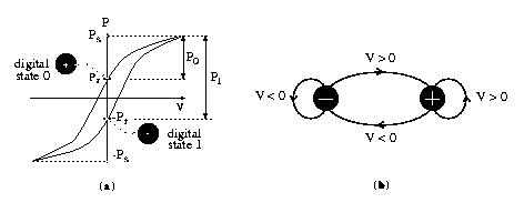
A circuit representation of the ZSTT Model is shown in in the following:
 C0(V0) and C1(V1) represent the two
nonlinear capacitors corresponding to the two binary states of
the FE capacitor discussed earlier. If the
binary state of the FE capacitor is 0, switches S01 and S12 are
closed while switches S11 and S02 are open.
In this case, the equivalent capacitance looking into the input
terminals is C0(V0). Meanwhile, a voltage
controlled voltage source, which is equal to Vi , is connected
to C1(V1) to initialize this capacitor for the
opposite binary state. For binary state 1, the states of the
switches are the reverse: switches S11 and S02 are
closed while switches S01 and S12 are open. Therefore, the
capacitance looking into the input terminals is
C1(V1), and the controlled source is connected to C0(V0)
for the similar reason mentioned above.
C0(V0) and C1(V1) represent the two
nonlinear capacitors corresponding to the two binary states of
the FE capacitor discussed earlier. If the
binary state of the FE capacitor is 0, switches S01 and S12 are
closed while switches S11 and S02 are open.
In this case, the equivalent capacitance looking into the input
terminals is C0(V0). Meanwhile, a voltage
controlled voltage source, which is equal to Vi , is connected
to C1(V1) to initialize this capacitor for the
opposite binary state. For binary state 1, the states of the
switches are the reverse: switches S11 and S02 are
closed while switches S01 and S12 are open. Therefore, the
capacitance looking into the input terminals is
C1(V1), and the controlled source is connected to C0(V0)
for the similar reason mentioned above.
If the initial binary state of an FE capacitor is known, its
subsequent binary states can be determined by
the applied pulse pattern. A binary state 0 remains unchanged in
response to a positive pulse as well as the
leading edge (falling edge) of a negative pulse. It
only changes on the trailing edge (rising edge) of the
negative pulse. A binary state 1 remains unchanged in response to
a negative pulse as well as the rising
edge of a positive pulse. It only changes on the falling
edge of the positive pulse.
The ZSTT Model can be easily implemented as an HSPICE macro-model
if the two nonlinear capacitors
in Fig. 10 are replaced by their piecewise linear approximations.
The switches can be replaced by voltage-
controlled resistors (VCRs) that exhibit high and low resistances
for the open and closed states of the
switches, respectively. The logic circuit shown:
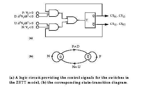 provides appropriate control signals for the
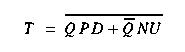
switches. The flip-flop toggles with the falling edge of T, where:
provides appropriate control signals for the
switches. The flip-flop toggles with the falling edge of T, where:
 The toggle flip-flop and the logic gates are all implemented in HSPICE.
One example of an input voltage pattern and its corresponding control signals
for the switches are
illustrated here:
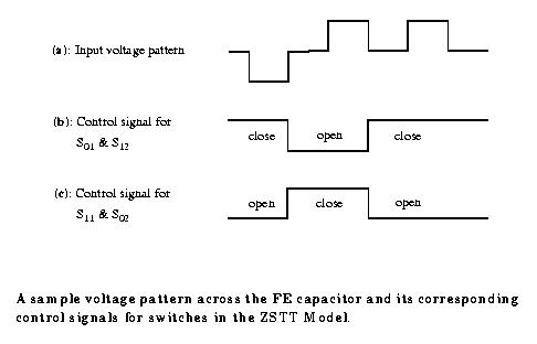 The initial binary state of the capacitor,
in this example, is considered to be 0.
Therefore, S01 and S12 are initially closed (CS01 = CS12 = High),
and the equivalent capacitance looking
into the input terminals is C0(V0). On the rising edge of the first
negative pulse, switches S11 and S02 are
closed (CS11 = CS02 = logic 1) and switches S01 and S12 are opened
(CS01 = CS12 = logic 0). In this case,
the capacitance looking into the input terminals is C1(V1).
This situation will be reversed again on the
falling edge of the first positive pulse.
The initial binary state of the capacitor,
in this example, is considered to be 0.
Therefore, S01 and S12 are initially closed (CS01 = CS12 = High),
and the equivalent capacitance looking
into the input terminals is C0(V0). On the rising edge of the first
negative pulse, switches S11 and S02 are
closed (CS11 = CS02 = logic 1) and switches S01 and S12 are opened
(CS01 = CS12 = logic 0). In this case,
the capacitance looking into the input terminals is C1(V1).
This situation will be reversed again on the
falling edge of the first positive pulse.
References:
[1] A. Sheikholeslami and P. Glenn Gulak, "Transient Modeling
of Ferroelectric Capacitors for Nonvolatile Memories", IEEE
Trans. on UFFC, Vol. 43, No. 3, pp. 450-456, May 1996
This work was supported by Nortel and the Natural Sciences and Engineering
Research Council of Canada.
Related Links:
We would appreciate
your comments and suggestions.
This page is maintained by Ali
Sheikholeslami. Created on July 4, 1997. Last modified on July 19, 2000.